Search

Silicon Valley at a glance

ASML Silicon Valley, located in San Jose, develops sophisticated software and metrology solutions for chipmakers, enabling ASML’s holistic lithography approach.

0123456789
0123456789
0123456789
0123456789

Year acquired Brion

0123456789
0123456789
0123456789
0123456789

Year acquired HMI

0123456789
k
+

Employees

2022 annual figures

0123456789
y
e
a
r
s

Average employee tenure

2022 annual figures

Enable third party cookies to play this video

Below you can enable third party cookies. Your choice will be saved and the page will refresh.

Our technology in Silicon Valley

At ASML Silicon Valley, we develop sophisticated software and metrology solutions, addressing escalating complexities encountered at smaller nodes. Local customer support and technology development also ensure superior system performance and service.

Read more


Holistic lithography

It’s no longer enough to optimize the various semiconductor manufacturing steps – IC design, mask creation, lithography, etch and deposition, and metrology – in isolation. In order to achieve optimum yield at smaller nodes, it requires a holistic approach. At ASML Silicon Valley, we integrate knowledge of the lithography systems with metrology and computational lithography to drive forward cost-effective shrink for chipmakers. 

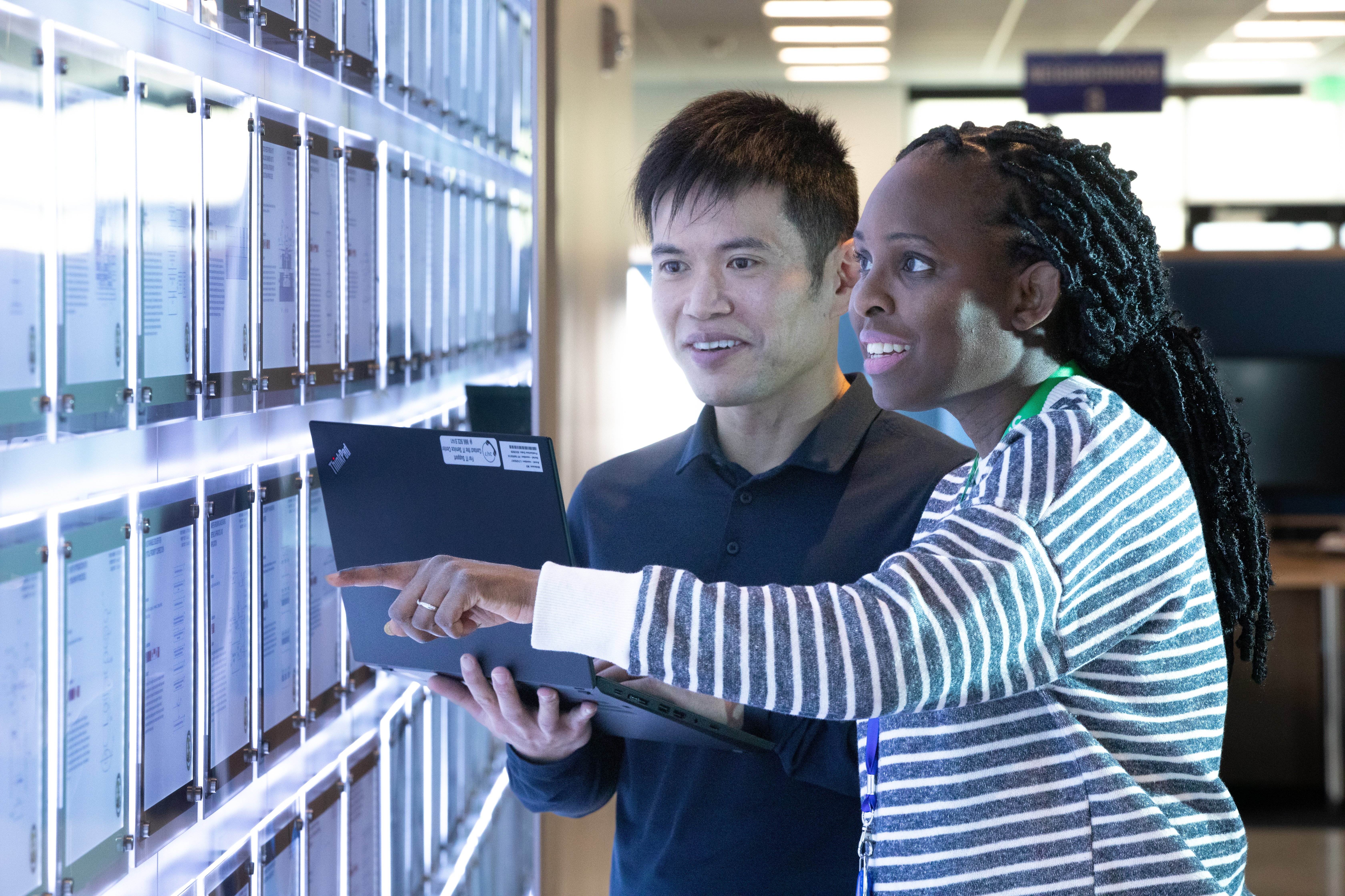
Software and metrology solutions developed at ASML Silicon Valley help enhance the manufacturability of designs through co-optimization of chip designs and scanner settings. Our colleagues in San Jose also develop solutions that optimize the performance of lithography systems, maximizing production yield and stabilizing systems in high-volume manufacturing.

A photo of Rafael Howell
Enable third party cookies to play this video

Sophisticated software models

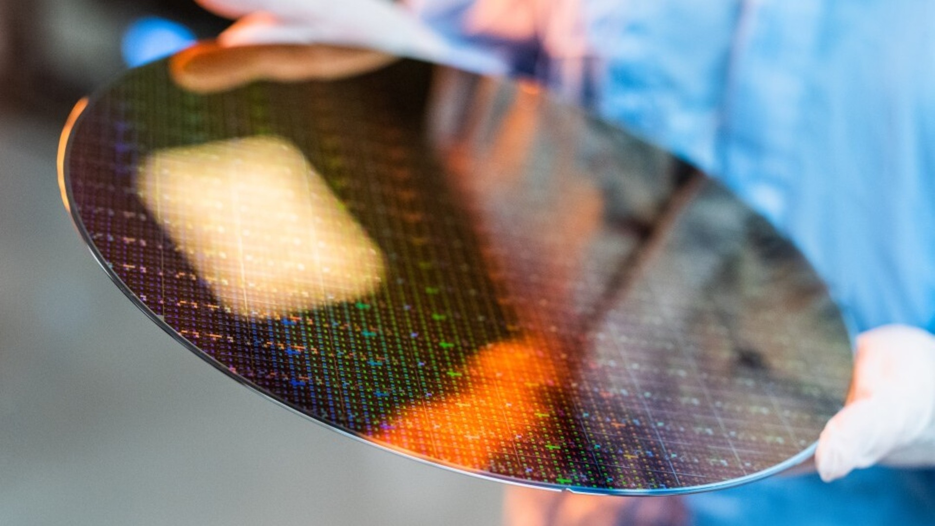
In an ideal world, we would pattern flawless squares and rectangles commonly seen in the blueprint of a chip design. However, after light passes through the reticle and the light-sensitive coating material is etched away, the pattern result on a silicon wafer can be quite different.


To address these changes to the chip, we develop sophisticated software models that capture various physical and chemical effects encountered throughout the lithography process. These models and numerical algorithms are used to accurately predict how a design pattern will be printed onto a silicon wafer and then optimize its shape to generate the image we want.

A photo of Gary Zhang
Enable third party cookies to play this video

High-performance computing applications

The complexity of the physics and sheer scale of the optimization problems faced at ASML Silicon Valley present challenges of their own. Today’s chips have billions of transistors, built up layer by layer with extreme precision, requiring the imaging of tens of billions of patterns that must be simulated and optimized within 24 hours – it’s an enormous, time-sensitive task. At ASML Silicon Valley, we develop innovative ways to speed up the model calculations. We harness the power of tens of thousands of computing cores to quickly process full chip blueprints – all without sacrificing accuracy. This is an iterative, computationally intensive process that requires the efficient and accurate utilization of a large-scale, distributed high-performance computing architecture.

E-beam technology

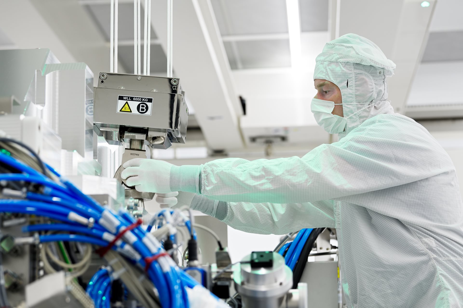
Today’s mainstream optical inspection technologies are reaching their resolution limits. With its high image resolution, e-beam metrology technology is becoming necessary to achieve accurate measurements and address shrinking margins of error. In Silicon Valley, we’re creating a new class of applications to ensure accurate wafer patterning performance and identify yield-related defects faster with higher accuracy across more wafers at the most advanced nodes.


E-beam technology uses a focused stream of electrons to measure chip geometries that are much smaller than those resolved by even the most advanced optical technology. ASML Silicon Valley brings additional metrology capability such as high-resolution imaging and voltage contrast that checks the integrity of the electrical properties of interconnect layers.


We use high-resolution e-beam images from e-beam metrology systems to improve our computational lithography models. These improved models are then used to enhance scanner control, leading to improved yield.

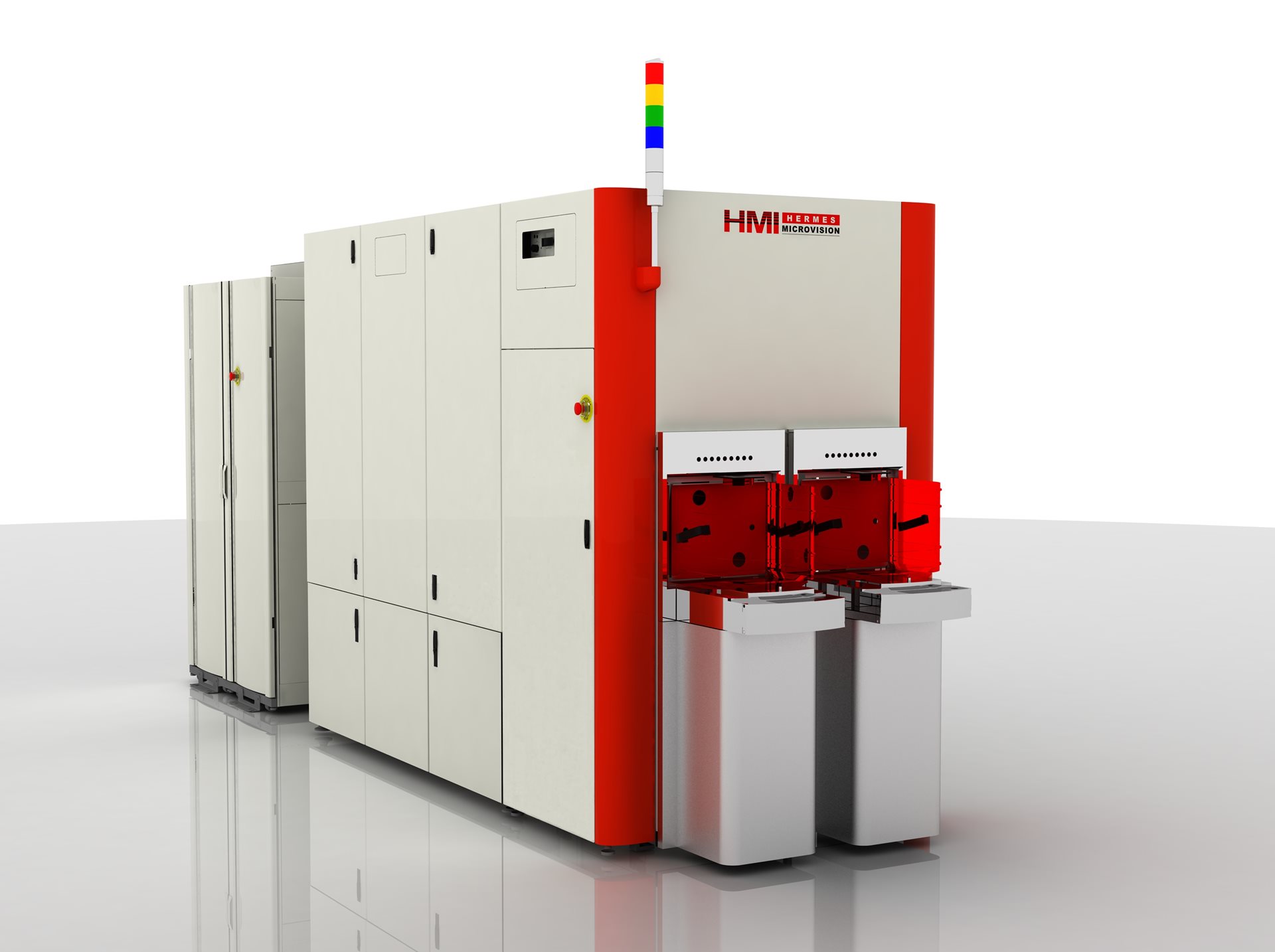
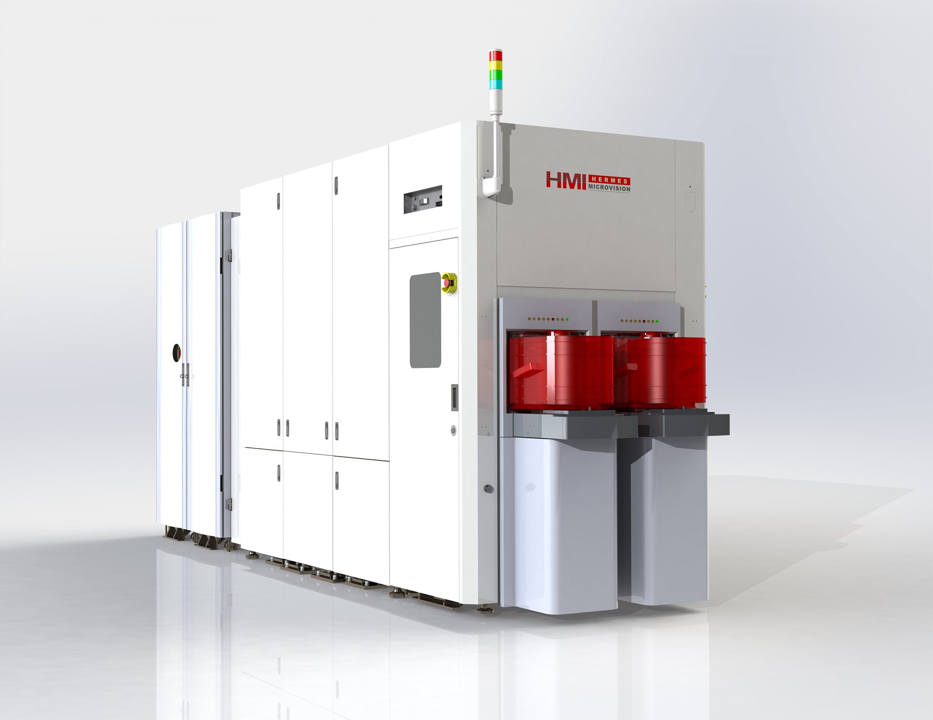
HMI eP5
Silicon Valley software illustration
Enable third party cookies to play this video

Below you can enable third party cookies. Your choice will be saved and the page will refresh.

Working and living in Silicon Valley

ASML Silicon Valley is located in San Jose, California – a dynamic area where technology and culture converge in a fast-paced, innovative environment. The third most populous city in California, San Jose ranks as one of the wealthiest cities in the United States.

Read more


Capital of Silicon Valley

San Jose, an entrepreneurial hub and home to the country’s most cutting-edge companies, is located within Silicon Valley in the United States. Silicon Valley is a region in the southern part of the San Francisco Bay Area that is renowned as the birthplace of the manufacturers who drove advancements in silicon-based transistors and integrated circuits. Silicon Valley is now synonymous with high-tech innovation, and the area receives a third of all venture capital investment in the United States.


With its large concentration of software, engineering, computer and microprocessor companies, you’ll find highly talented people with technical skills that are hard to match anywhere else. The best and brightest minds in engineering, technology and science work right in San Jose.

Northern California lifestyle

The Bay Area offers a rich and varied landscape and culture: explore its dramatic coastlines and Redwood forests or visit historic places such as San Francisco, Napa Valley and Sonoma wine country. Combined with its ‘eternal summers’ and mild weather, residents and visitors enjoy a wide range of activities including surfing, hiking, visiting museums and aquariums, and sampling diverse cuisine.


Public transportation such as Caltrain and the BART (Bay Area Rapid Transit) offer easy access in and around the Bay Area, connecting both urban and suburban areas such as Berkeley, Oakland and Walnut Creek. For those willing to hop in a car for a longer drive, there are opportunities to explore Yosemite National Park, Half Moon Bay and Monterey Bay.

Silicon Valley

Software heroines

Leading the way for women in ICT at ASML

Read about Mingjing Zhao, a senior software quality assurance manager at ASML in Silicon Valley, and other women as they pursue their dreams in computer science and software engineering at ASML.

An illustration of a woman wearing a red cape standing on top of a skyrise building made of zeros and ones.

ASML's Glassdoor rating

Powered by Glassdoor
4.2/3145 ratings

Culture & Values

3.8

Work/life balance

3.7

Senior Management

3.4

Compensation and Benefits

3.9

Career opportunities

3.8

Diversity & Inclusion

4.3

Meet Franklin Wong, applications group lead

Meet Roshni Biswas, R&D manager

Meet Shubhangi Alande, software engineer

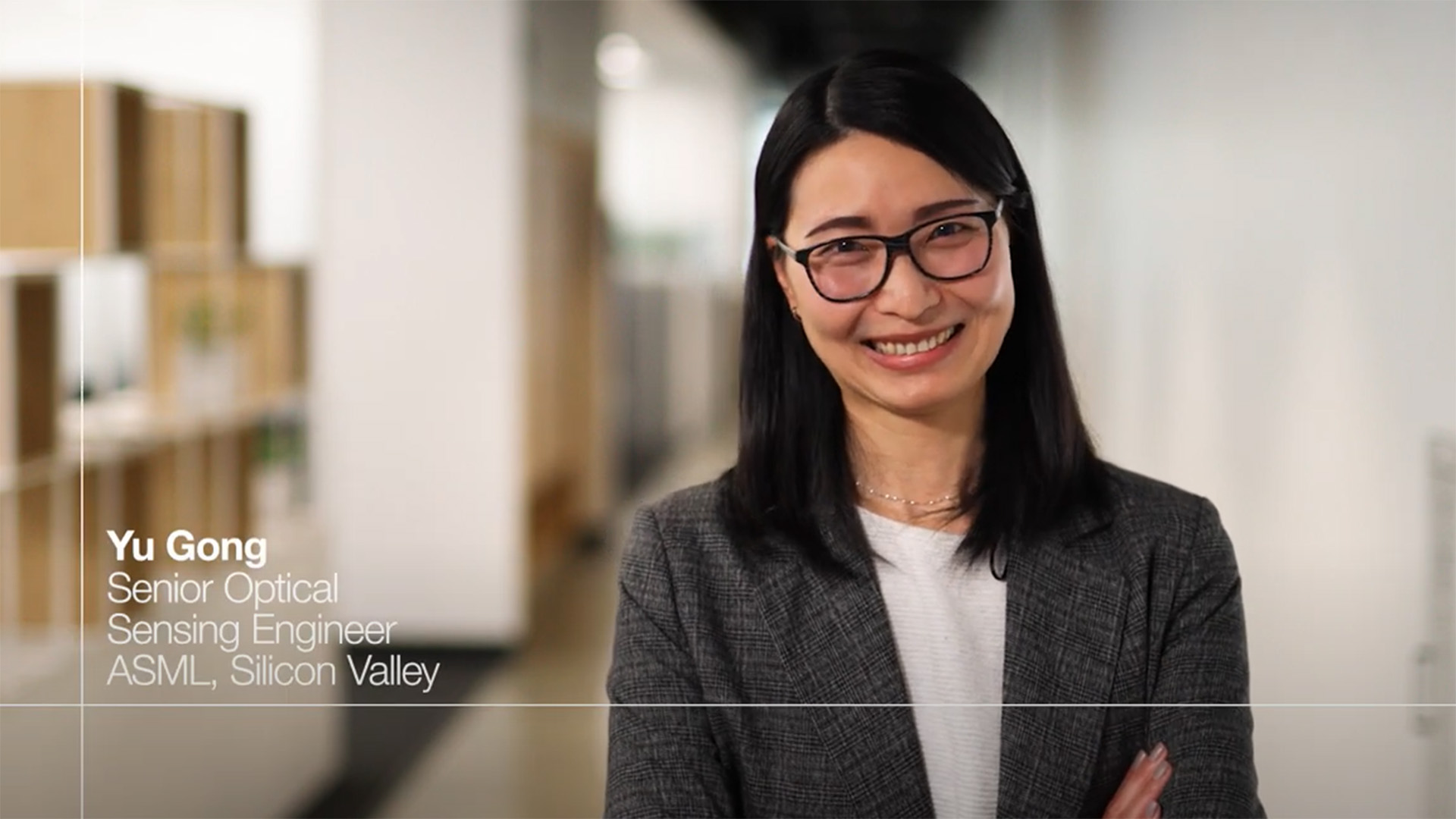
Meet Yu Gong, senior optical sensing engineer
Visit ASML in Silicon Valley

80 West TasmanSan Jose, California 95134United States+1 408 597 8600