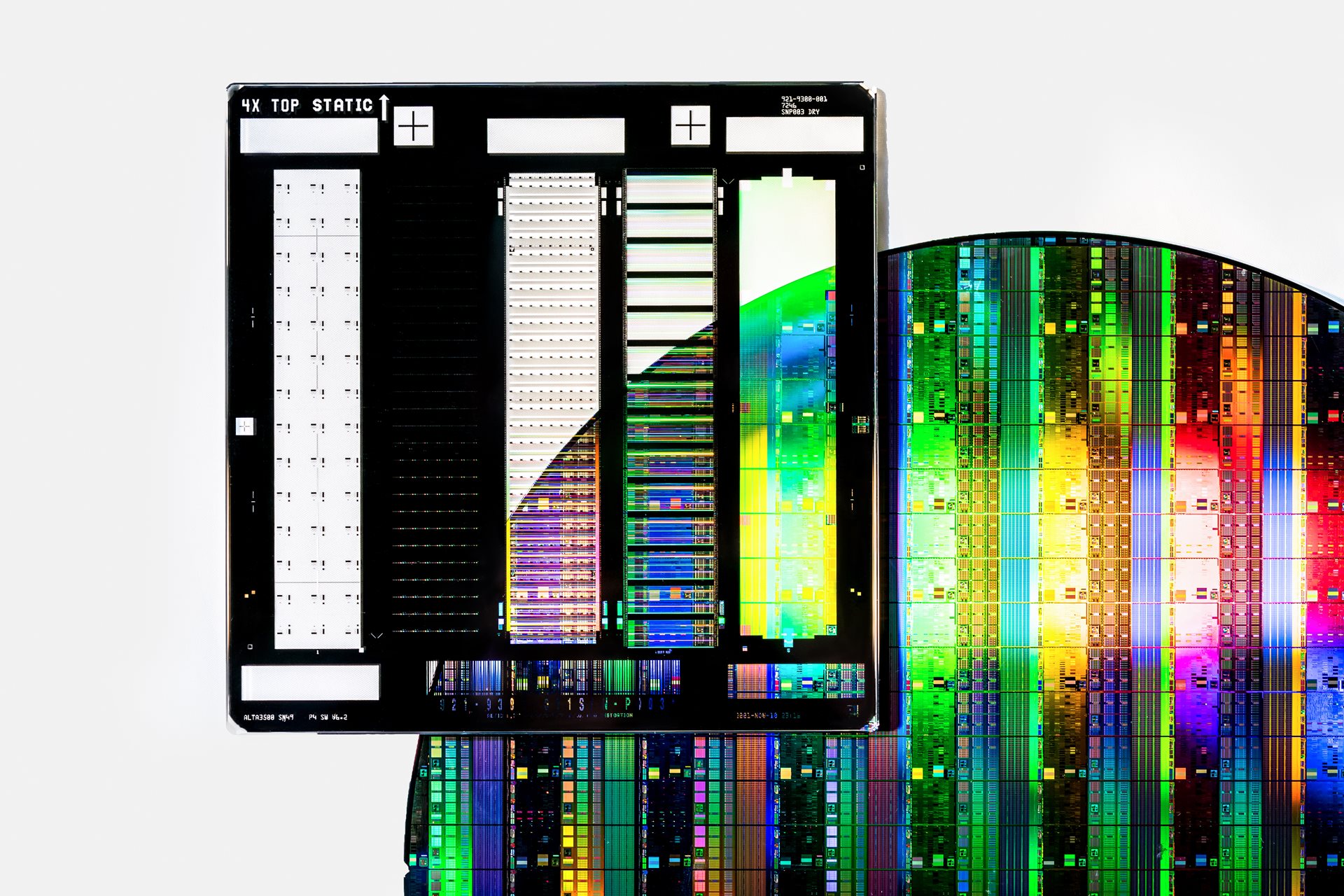
Together with our computational lithography and patterning control software solutions, our wafer metrology and inspection portfolio helps chipmakers achieve the highest yield and best performance in mass production of semiconductor chips.
YieldStar optical metrology
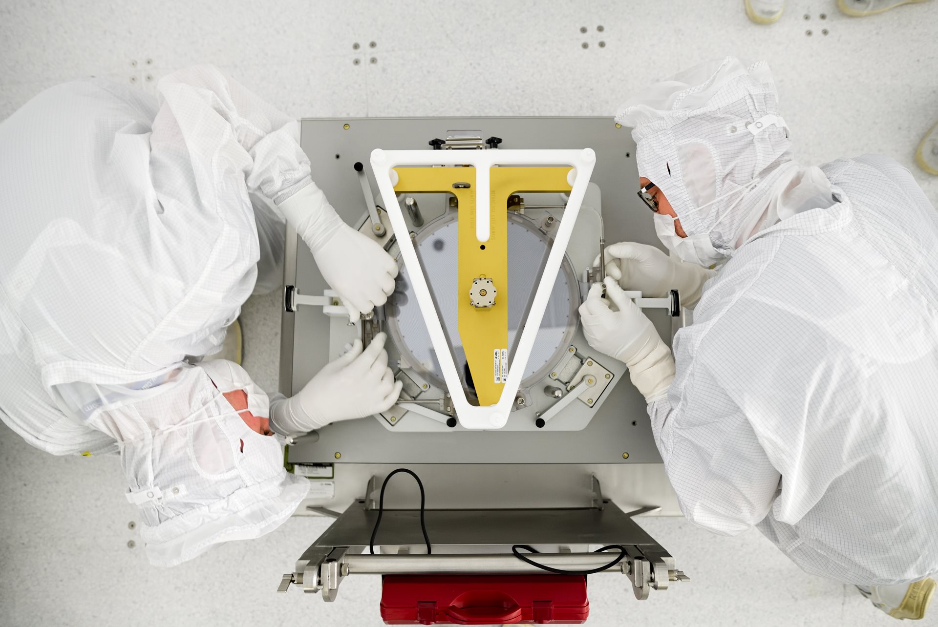
Our YieldStar optical metrology solutions for the semiconductor industry can quickly and accurately measure the quality of patterns on a wafer.
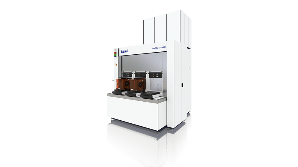 YieldStar 1385
Fast, accurate optical metrology of in-device overlay for post-etch process monitoring
.png?h=1080&iar=0&w=1920) YieldStar 1390
YieldStar 1390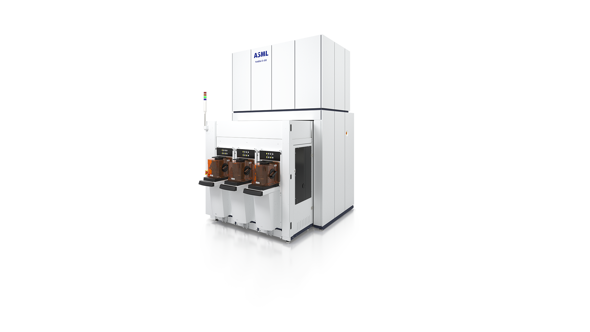 YieldStar 500
The YieldStar 500 is a stand-alone optical wafer metrology system for measuring pre-etch overlay leveraging ASML’s innovative TWINSCAN stage.
E-beam metrology and inspection
Our HMI e-beam solutions help to locate and analyze individual chip defects amid millions of printed patterns.
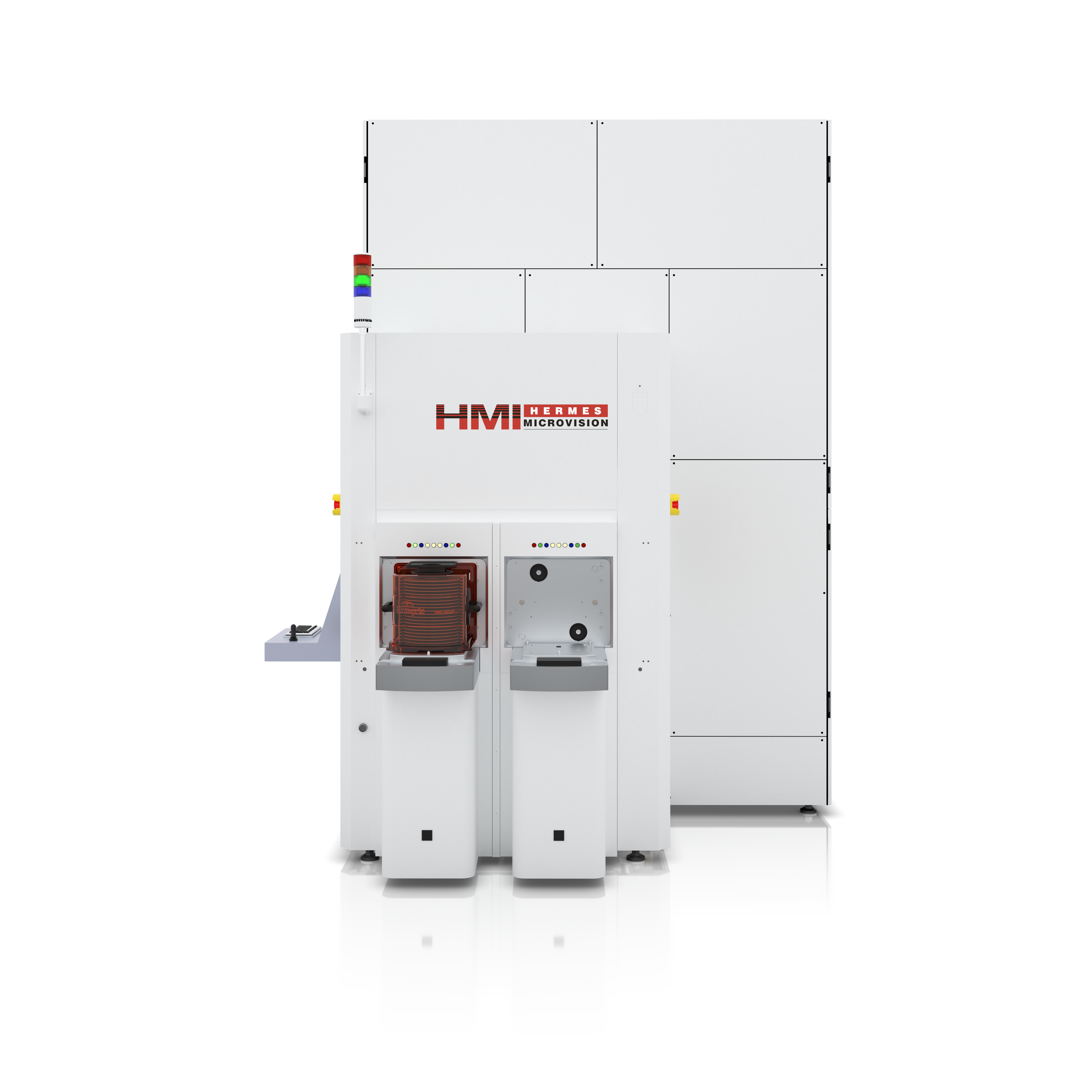 HMI eScan 1100
The first generation multiple e-beam (multibeam) wafer inspection tool for in-line defect inspection applications
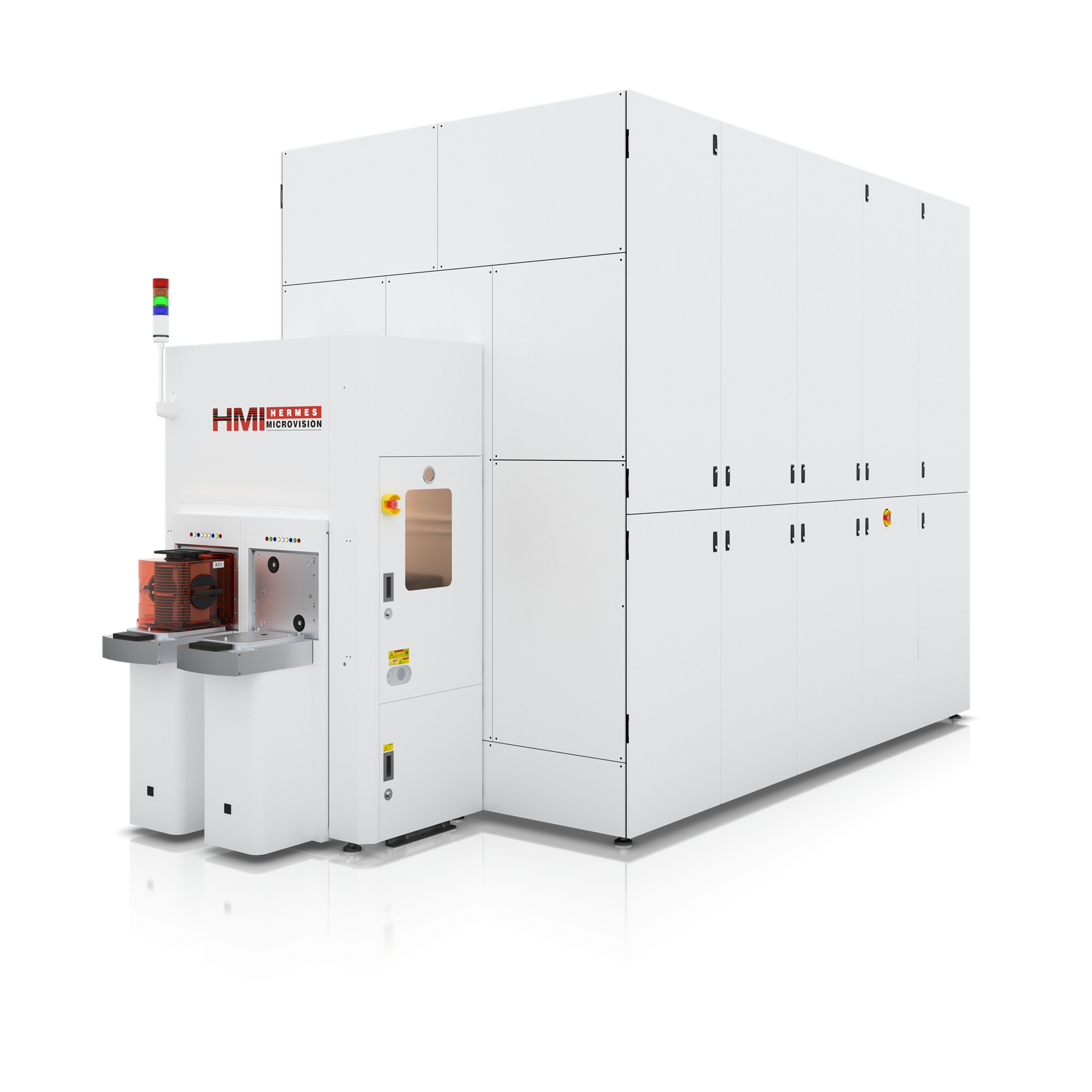 HMI eScan 1000
The world’s first multiple e-beam (multibeam) wafer inspection tool.
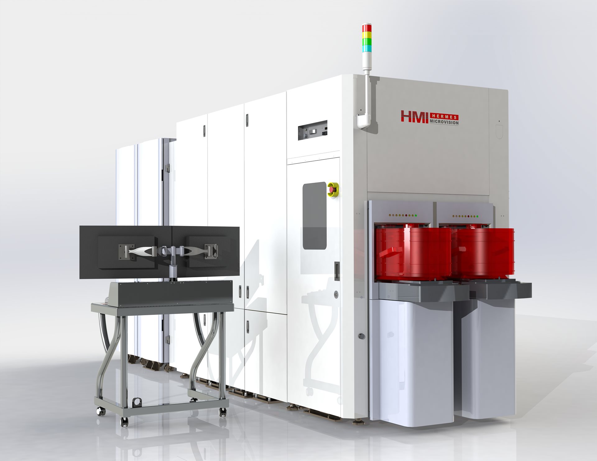 HMI eScan 600
Flexible e-beam inspection solution that detects multiple defect types in one system.
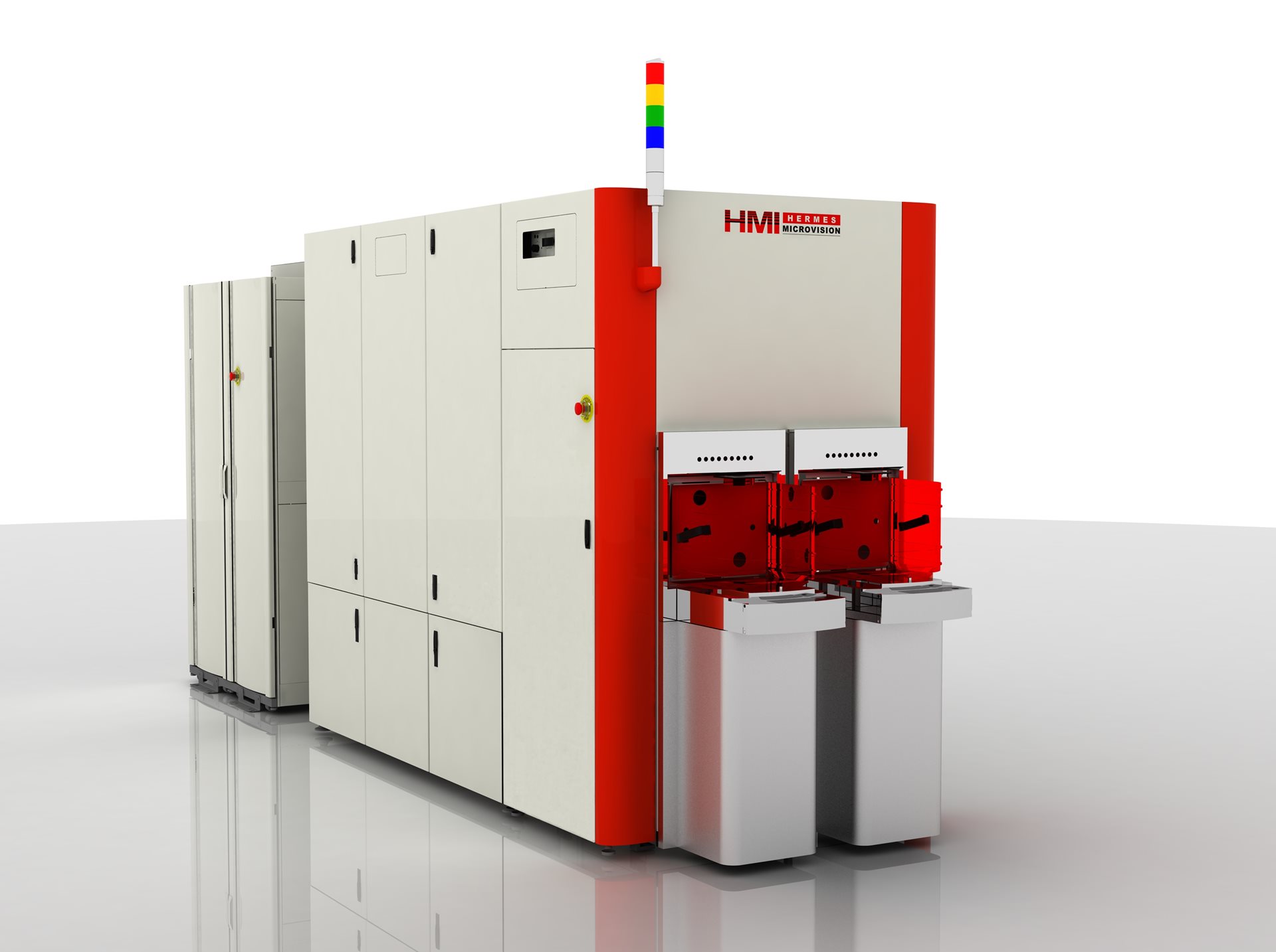 HMI eP5
Our highest resolution e-beam system offers CD metrology and defect detection for chip development and production monitoring.