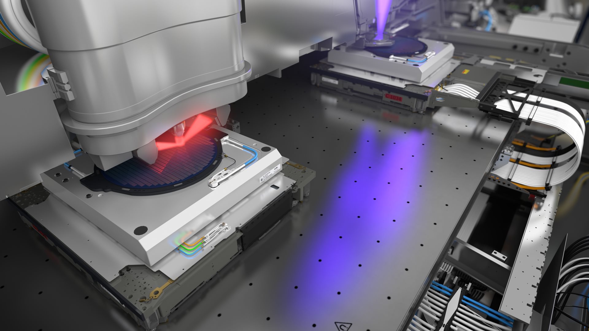
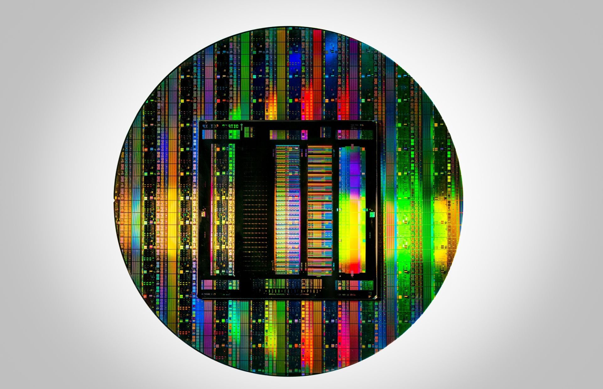
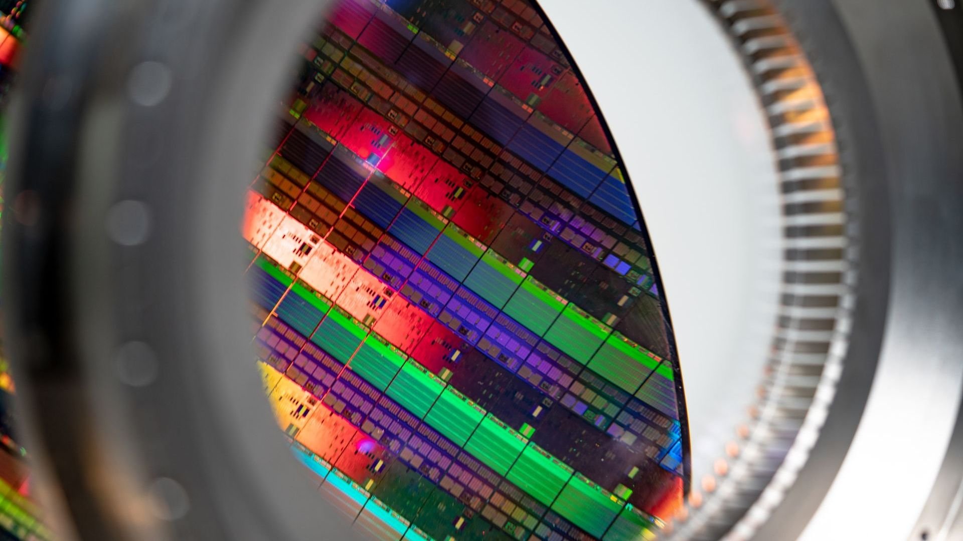
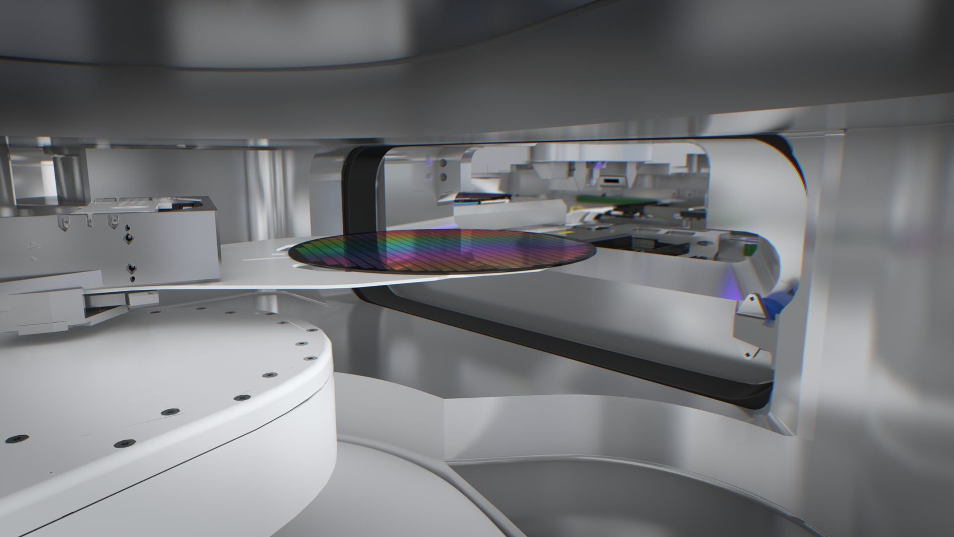
Microchips are made by building up complex patterns of transistors, layer by layer, on a silicon wafer. ASML’s lithography systems are central to that process.
A lithography (more formally known as ‘photolithography’) system is essentially a projection system. Light is projected through a blueprint of the pattern that will be printed (known as a ‘mask’ or ‘reticle’).
With the pattern encoded in the light, the system’s optics shrink and focus the pattern onto a photosensitive silicon wafer. After the pattern is printed, the system moves the wafer slightly and makes another copy on the wafer.
The science behind the chip
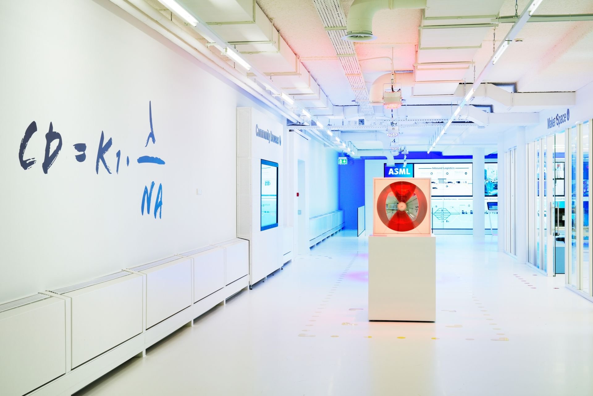 The Rayleigh criterion
Learn the equation that determines just how small the transistors on a microchip can be.
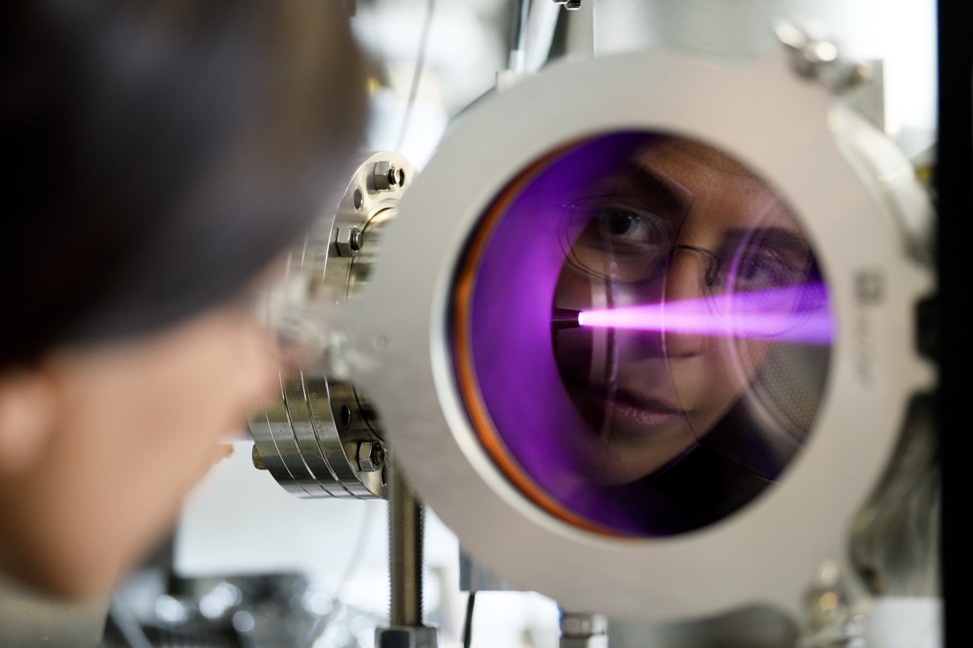 Light & lasers
From visible blue light to invisible extreme UV light, our lithography machines keep innovation in light and lasers moving forward.
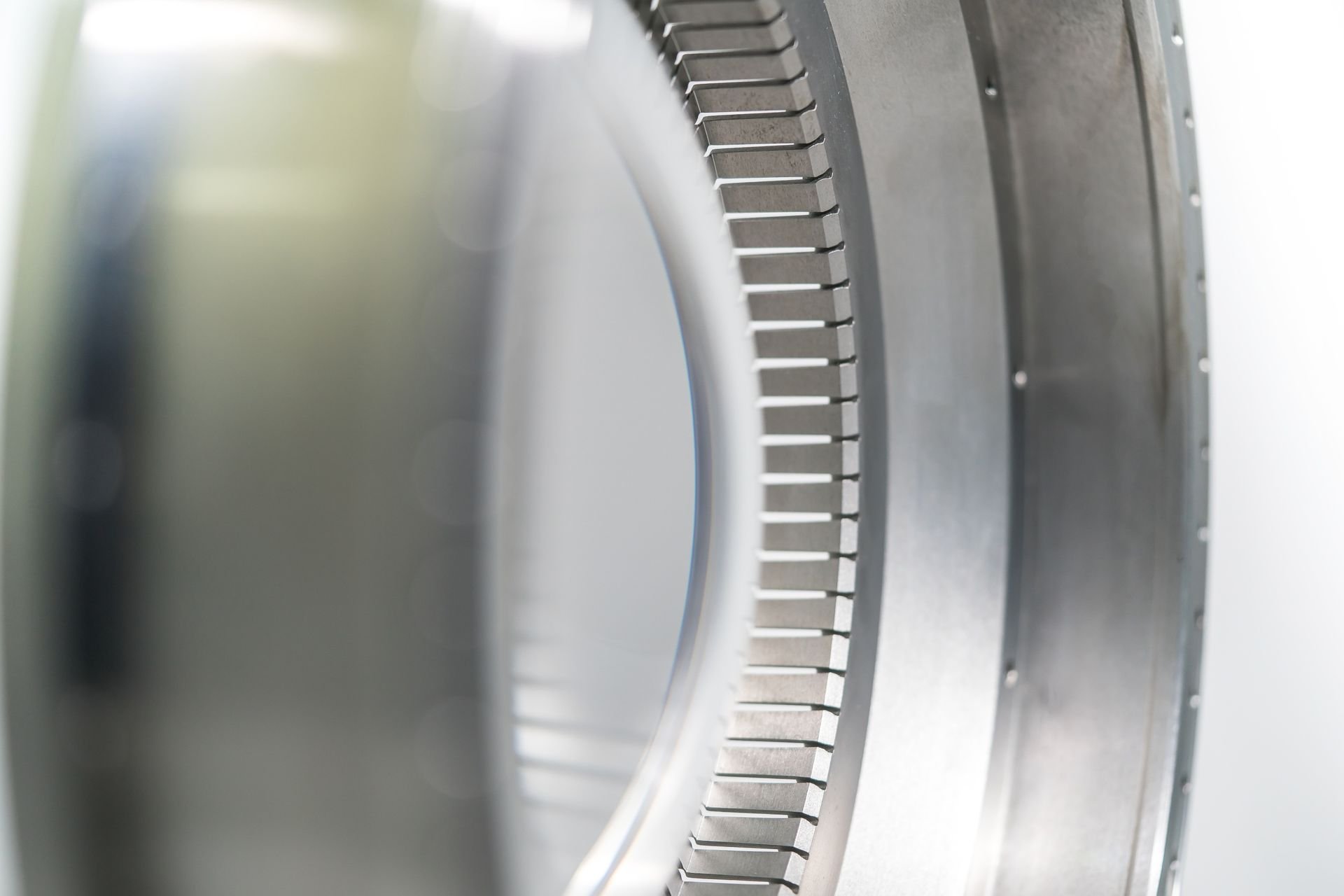 Lenses & mirrors
The complex optical systems in our lithography machines reduce the image to be printed on a wafer to the nanometer level.
 Mechanics & mechatronics
Our lithography machines feature some of the world’s most advanced, precision-engineered mechanical and mechatronic systems.