As an electrical engineer at ASML, you’ll work on intricate machines with diverse and complex electronics.
Building the electronics used in everyday devices
At ASML, we manufacture chipmaking machines that power all of our modern devices – laptops, phones, cameras, cars, medical devices and more. Our electrical engineering team designs, develops and maintains all the electrical systems and components of the most advanced lithography machines in the world. This team spans a range of competencies including electro-mechanical, firmware and design, electronics integrators and architects and PCB (printed circuit board) layouts.

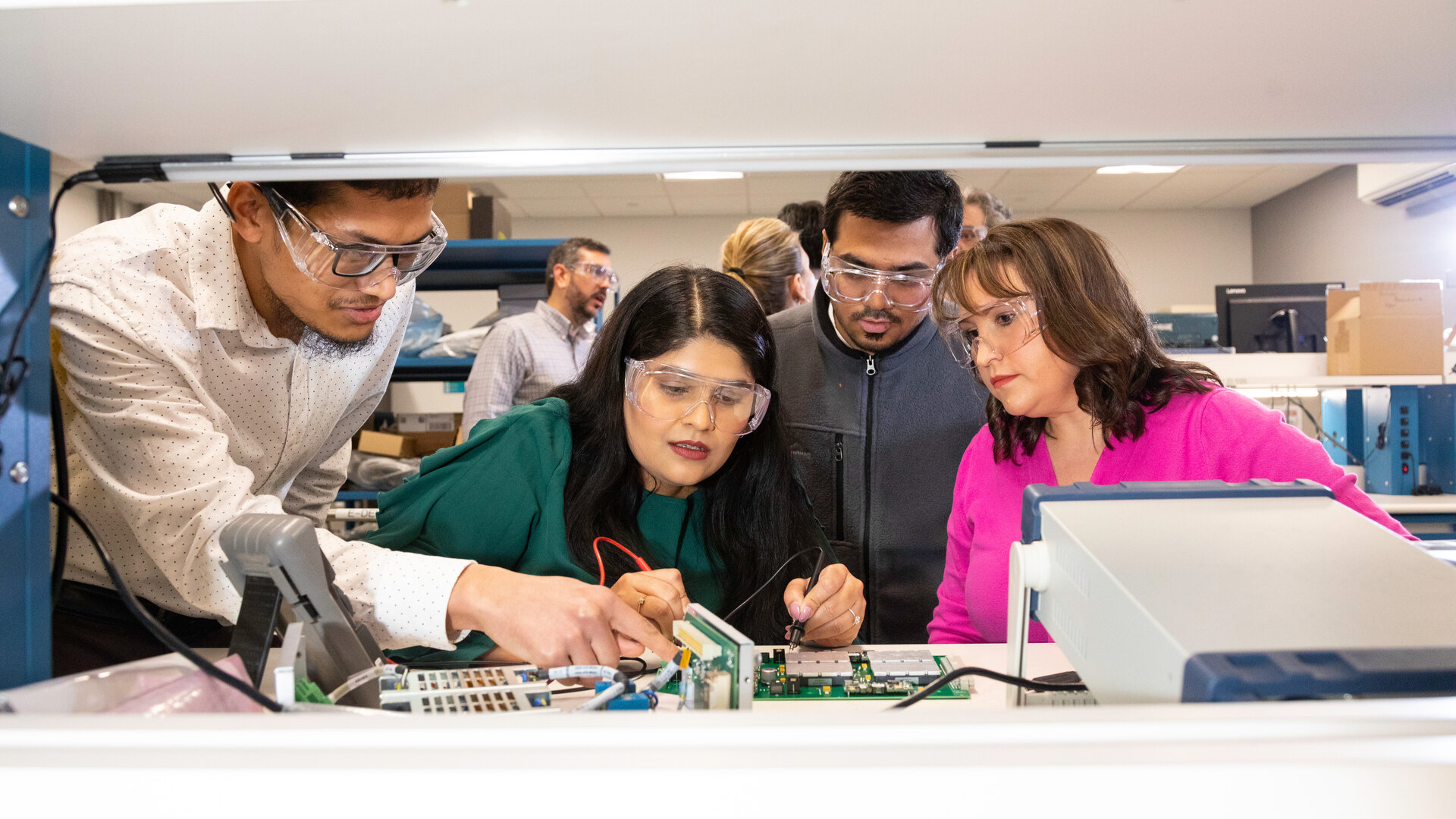
As part of the electrical engineering team, you’ll deliver electronic and electrical designs for the entire development process from conceptualizing design to prototyping, volume manufacturing and initial integration through qualification. You’ll design and optimize electrical circuits including analog and digital circuits through simulation and PCB layout. You’ll also evaluate and select electrical components such as integrated circuits, sensors, and power devices to increase performance, reliability, cost, and availability. You’ll collaborate with multidisciplinary teams including mechanical engineers and software engineers on the electrical infrastructure, detailed electrical design and drawings and documents to ultimately come up with the best solution.
Overall, our electrical engineering team plays a crucial role in designing and maintaining the electrical systems that enable high-precision and throughput of the lithography processes of our chipmaking machines.

Inside the EUV machine
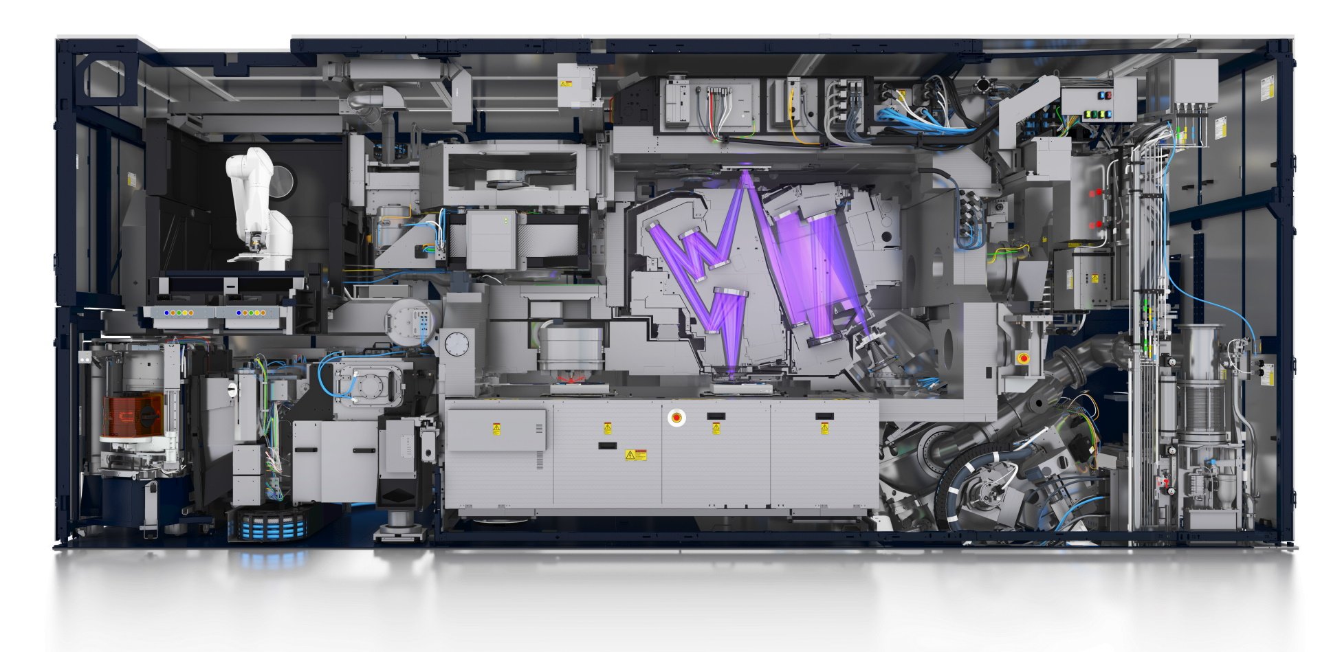
Analog and digital designs, cabling and layout, sensor electronics, power electronics and motion control all come together in our extreme ultraviolet lithography machines.
It's just one challenging area in which our electrical engineers work. EUV light is generated in the source module and then sent into the illuminator, which controls the light beam. The light reflects off the reticle (the mask containing the pattern that is printed on the chip) and is then focused by the projection optics to ‘expose’ the silicon wafer.
The wafers are mounted on tables in what’s called the 'wafer stage'. The stage moves two wafer tables at the same time, each holding a silicon wafer. While one wafer is being exposed to the light, the other is measured by the machine’s metrology sensors to optimize alignment. The wafer tables move electromagnetically, allowing frictionless acceleration up to 7 g.


Meet Diana Mudeer, Test Technician
Meet Timea Kane, Senior Design Engineer
Browse electrical engineering jobs
Become part of progress as an electrical engineer at ASML.
Want to be alerted for new jobs?
Create job alert

