EUV light wavelength
Resolution
Projection optics
Wafers per hour
Key features & benefits
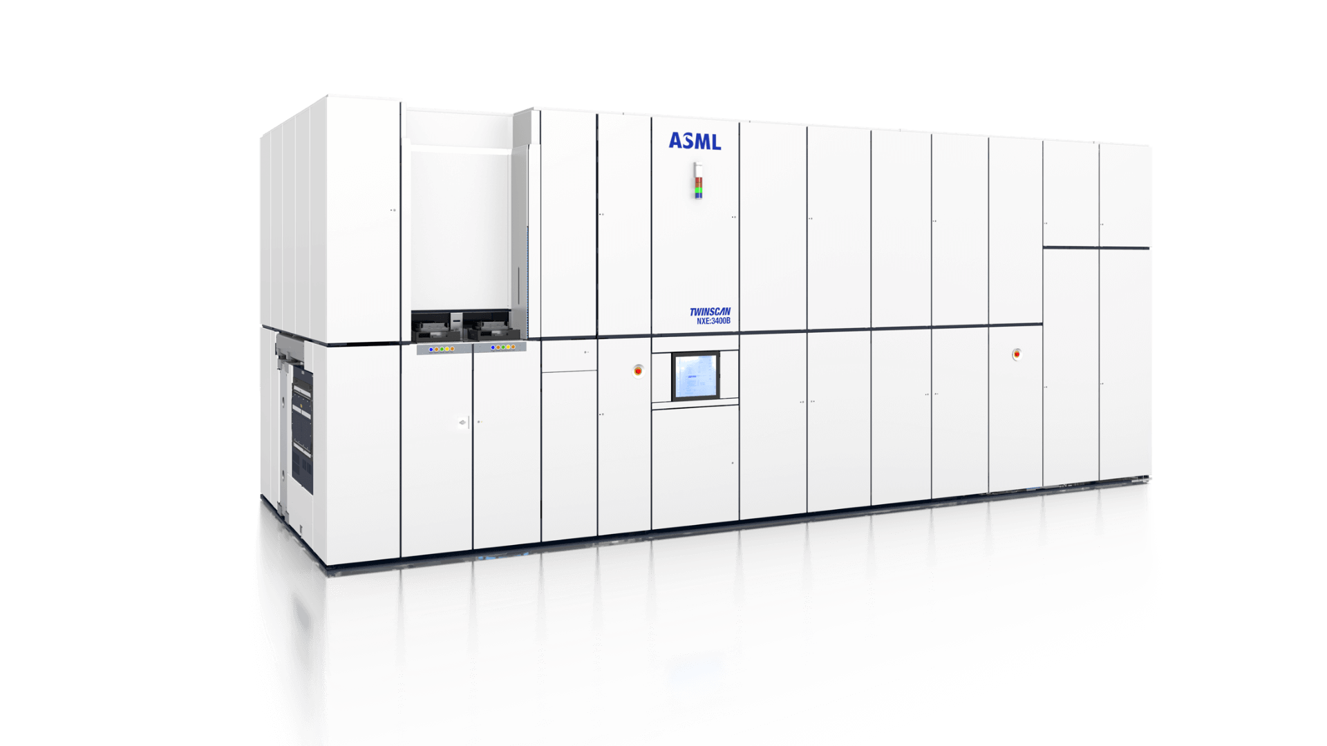
The TWINSCAN NXE:3400B supports EUV volume production at the 7 and 5 nm nodes.
Combining productivity, excellent image resolution, matched overlay to EUV NXE and ArFi NXT tools and focus performance, the NXE:3400B provides lithography capability complementary to ASML’s ArFi technology.
01. Productivity
The 300 mm wafer throughput target specification for the NXE:3400B is larger than or equal to 125 wafers per hour under the following conditions: Dose: 20mJ/cm2, die size: 26 x 33 mm, 96 shots.
02. Optics
The TWINSCAN NXE:3400B Step & Scan system includes Zeiss 4x reduction EUV optics with a Numerical Aperture (NA) of 0.33 and a maximum scanned exposure field size of 26 x 33 mm.
The NXE:3400B illumination is designed to extend the off-axis illumination imaging capabilities with advanced freeform pupil shaping for low-k1 imaging at optimal productivity. In addition, the operating range sigma was increased from 0.2 – 0.9 to 0.06 – 1.0 to make optimal use of the projection lens imaging capabilities.
03. Imaging performance
The NXE:3400B can achieve a dedicated chuck overlay of 1.4 nm and a matched-machine overlay of 2 nm. Overlay accuracy is measured over the whole field and over the whole wafer.
Wafer alignment occurs at the measurement position with target detection using SMASH alignment sensors with ASML's proven phase grating alignment technique.
The NXE:3400B incorporates the same level sensor as its predecessor the NXE:3350B, based on UV light source that reduces height process dependencies from wafer film stack variations.


