Press release - Albany, NY, August 26, 2004
Albany NanoTech of the University at Albany at the State University of New York announced today that its College for Nanoscale Science and Engineering (CNSE) has installed and begun qualifying for 300 mm wafers using the world’s first 193 nm pre-production immersion lithography system.
The activity brings together worldwide technical expertise and state-of-the-art resources in immersion lithography science and technology from ASML, IBM, and Tokyo Electron Limited (TEL) to the ever-expanding 300 mm wafer nanotechnology R&D complexes of Albany NanoTech, further establishing it as one of the most advanced university complexes in the world.
"ASML’s early lead in immersion is due to the company’s commitment to technology leadership. Our development strategy puts ASML’s first testing tools in the hands of customers to speed the proliferation of immersion technology," said Martin van den Brink, executive vice president, marketing and technology, ASML. "This alliance with Albany Nanotech and CNSE allows us to innovate with existing customers AMD, IBM and Infineon as well as business collaborator TEL within a world-class university research complex. In the future, the introduction of new technologies will require this type of early collaboration. Teamwork drives equipment suppliers to deliver total solutions and customers to deliver complete equipment applications."
"The technology and expertise from ASML and TEL combined with the research know-how of IBM represent a critical milestone in enhancing Albany NanoTech’s status as an international leader in nanotechnology development and education. Resulting industry-university programs will play a significant role in the strong lithography programs at CNSE, ensuring an unparalleled research capability that will provide immediate scientific and technical solutions to our semiconductor industry customers," said Alain E. Kaloyeros, PhD, vice president and Chief Administrative Officer of CNSE and professor of nanoscience at UAlbany. "This achievement was made possible through the support of Governor Pataki, Speaker Silver, and Senator Bruno and their ongoing investments in New York’s high-tech economy."
Recent research has moved immersion lithography to the forefront of the semiconductor industry as a promising, next generation technology. It requires the gap between the lens of the exposure tool and the silicon wafer to be filled with a liquid, such as water, instead of air, to enhance resolution performance. The market for immersion lithography tools is projected to go from zero to $230 million by 2005, according to industry analysts.
"CNSE’s acquisition and rapid installation of the pre-production 193 nm immersion system is an impressive industry first and demonstrates the continued commitment of Albany NanoTech and New York State to its industrial partners," said Dr. John E. Kelly III, senior vice president, technology, IBM Systems and Technology Group. "This achievement will provide the early learning to enable continued leadership in the development of future nanoelectronic devices."
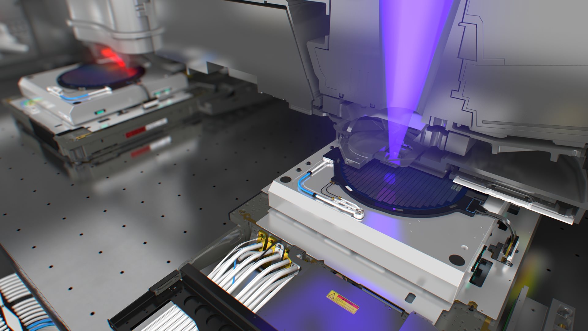
Under the program, researchers and engineers from CNSE, ASML, IBM and TEL will work jointly on site at Albany NanoTech to demonstrate and optimize materials and processes for emerging 193 nm immersion lithography on a clustered 300 mm wafer scanner-track platform. The integrated platform consists of two components: the ASML TWINSCAN AT:1150i scanner and a Tokyo Electron Limited CLEAN TRACK LITHIUS coater/developer system.
The collaboration between business, higher education and government at CNSE has created an epicenter of nanoelectronics research which is attracting unprecedented investment and cooperation, as well as providing an environment in which the partners receive early access to some of the most advanced semiconductor tools and equipment available today. As part of their ongoing work with the CNSE, AMD and Infineon also will work with IBM and CNSE in the use of the AT:1150i for the development of immersion lithography processes and applications.
"AMD is committed to pioneering research in immersion lithography, so we’re excited to see the first 193 nm immersion lithography system installed at Albany NanoTech," said Dr. David Kyser, director of external research at Advanced Micro Devices. "AMD scientists are already working closely with scientists at the College of Nanoscale Science and Engineering, and the addition of leading-edge tools can only enhance our already fruitful engagement."
"Putting the first pre-production 193 nm immersion lithography system at Albany NanoTech enables nanoelectronics innovators like Infineon to advance their leading-edge R&D programs more efficiently, ultimately benefiting our customers and the industry as a whole," said Wilhelm Beinvogl, CTO Memory Products Group at Infineon. "This new tool is a significant addition to Albany NanoTech’s already extensive lithography research infrastructure with participation of a sizable Infineon engineering group."
Albany NanoTech complex, as the home of CNSE and the New York State Center for Excellence, enables programs that cover the entire spectrum of nanoelectronics industry needs, from long-term innovative research and development, to workforce education and development, to product prototyping and commercialization. The Center for Excellence in Nanoelectronics is supported by investments from New York State and the IBM Corporation. Albany NanoTech also hosts the research facilities for International Sematech North R&D Center and the Tokyo Electron Limited Technology Center America.
About ASML
About Albany NanoTech


