5-minute read - by Kate Brunton, April 20, 2023
Chips are in demand – especially chips made using ‘dry’ DUV lithography equipment. How is innovation in this more mature sector helping to drive advances in society, and how is ASML helping chipmakers to stay on top of the demand for chips?
Microchips are everywhere and there are many different types. Every electronic device or system contains at least one chip, but it can be many more – a modern car, for example, can have over a thousand. And chips are also in less obvious places, such as your bank card.
Chips vary in complexity, depending on the task they need to fulfil. The simplest types of chips can be made with more mature lithography technology, whereas manufacturers of the most complex chips need the latest EUV lithography systems to produce them.
What are the different types of microchips?
There are two major ways to categorize microchips: by functionality and by type of integrated circuitry. Looking at circuitry, a chip can be analog, digital, or mixed. The difference between analog and digital function has to do with the electric signals they process. In digital chips, the signals are binary. In analog chips, the signals are continuous, meaning they can take on any value within a given range, and they use more traditional circuit elements (resistors, capacitors and occasionally inductors).
Looking at functionality, there are four main categories: Logic chips, Memory chips, application-specific integrated chips (ASICs) and system-on-a-chip devices (SoCs). The two most common types of chips, Logic chips and Memory chips, are digital: they manipulate and store bits and bytes using transistors. Logic chips, such as CPUs (central processing units), are the ‘brains’ of electronic devices – they process input, store data, and output results.

Memory chips store information. ‘Volatile’ Memory chips, such as DRAM, are the ‘working memory’ chips that save data only while the device’s power is turned on, whereas ‘non-volatile’ Memory chips such as NAND Flash save data even after the device is turned off.
ASICs are simple, single-purpose chips used for performing repetitive processing routines such as scanning a barcode. And finally, an SoC is essentially an integrator chip. It’s a relatively new type of chip that combines many chips and circuits in a single chip and may integrate things such as graphics, audio, camera, video and Wi-Fi.
What’s so special about 'simpler' chips?
Semiconductor technology has evolved a lot since the microchip was first invented in the late 1950s. As time progressed, manufacturers were able to create increasingly powerful chips by shrinking the size of the printed circuitry so as to fit more transistors on a chip. Over the years, ASML has developed lithography machines that can print smaller and smaller features by using shorter light wavelengths and increasing the numerical aperture of the machines’ optics.
Today’s most advanced chips – like the Logic chip in Apple’s iPhone 14 or the graphics chip in Nvidia’s RTX 4090 – can have as many as 100 layers of extremely tiny electronic features. Printing the most sensitive layers of these chips requires ASML’s most advanced technology: extreme ultraviolet (EUV) lithography, which uses light with a wavelength of 13.5 nm.
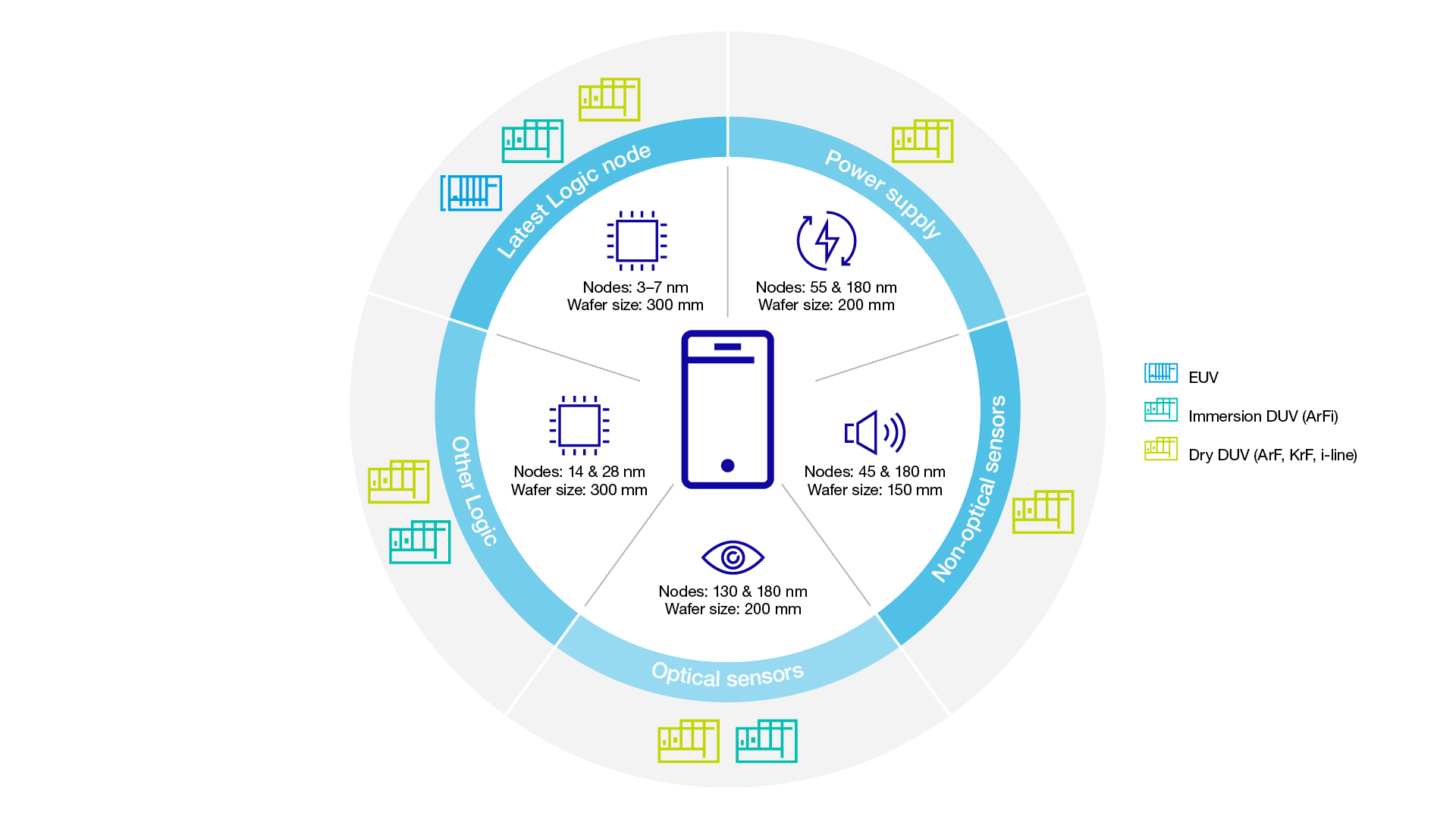
But many chips consist of fewer layers and don’t require the smallest features. Still, they perform crucial functions, including regulating the power coming into and moving through the device and sensing physical inputs such as light and sound. These ‘simple’ chips are produced using older lithography systems, including ASML’s ‘dry’ deep ultraviolet (DUV) lithography machines, which use light with wavelengths between 193 and 365 nm.

What is dry lithography and why is it important?
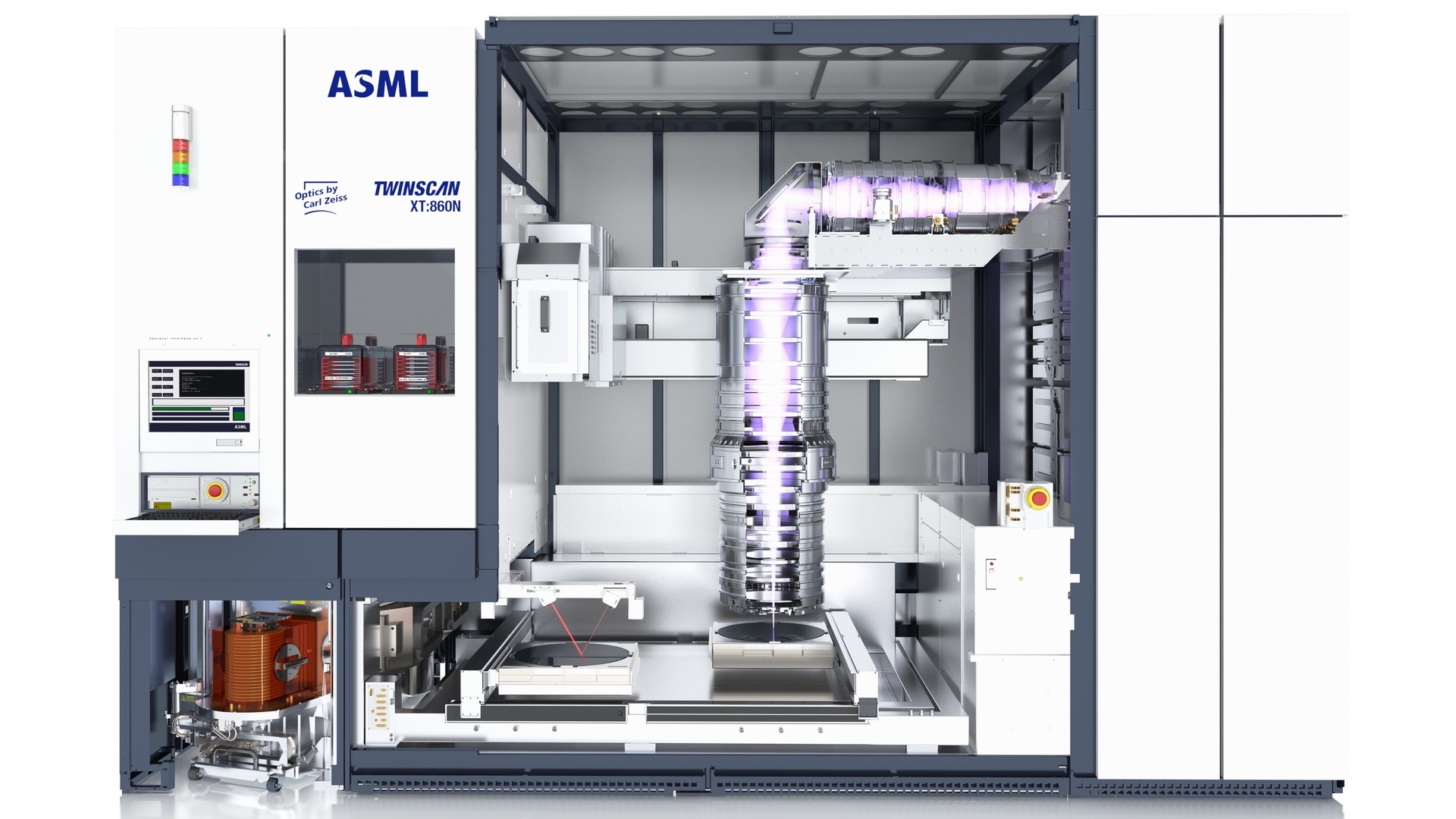
Dry lithography is the technological predecessor of ASML’s immersion lithography, which was developed in 2003 and increases a lithography machine’s resolution by adding a layer of water between the optics and the wafer. The term includes ASML’s PAS, TWINSCAN XT DUV and some TWINSCAN NXT DUV systems.
“Chips from 20 years ago made on dry lithography machines are, in some ways, less advanced than today’s chips,” explains Jeroen de Groot, director of DUV XT product marketing at ASML. “But that doesn’t mean that they aren’t in demand. In fact, the demand for simpler chips is growing fast.”
Thanks to this heightened demand for simpler chips, ASML’s dry lithography equipment is becoming more popular. Sales of new and refurbished machines have increased, and chipmakers are using their installed dry ASML lithography equipment more heavily.
What’s driving today’s demand for simpler chips?
The current demand is partly driven by COVID-related changes in company and consumer behavior, but it also reflects increasing digitalization around the globe. The connected world, climate change and resource scarcity, and social and economic shifts such as urbanization are all examples of trends driving the demand for all microchips, especially simple chips.
“It’s also important to remember that even though the latest gadgets may rely on EUV and immersion DUV lithography for some of the chips inside the device,” says Jeroen, “most chips, and even most of the layers on advanced chips, are printed on dry lithography machines.”
How is ASML helping chipmakers to meet demand?
ASML is tackling the demand for chips by researching and developing improvements for the next generation of dry lithography equipment, optimizing and upgrading machines already in our installed base, and buying back and refurbishing older PAS and XT systems. (Almost every single ASML lithography system sold is still in use at a customer fab, which means it’s important for us to focus on durability, repairability and re-use in our product designs.)
Helping our dry lithography customers often involves creating tailored solutions. Erik van Kouwen, vice president of DUV product management at ASML, explains: “For our customers in the mature markets, it’s more about diversity in all different directions, which means the specific needs of each customer may vary. It's advanced technology innovation in a new direction: instead of supporting shrink, we’re supporting new materials, wafer sizes and packaging.”
For example, ASML is building new lithography machines on dry product platforms that can handle different wafer sizes and thicknesses. This functionality is especially relevant for producing power supply chips like the ones found in smartphones, laptops and electric cars. (Power supply, or power management, chips provide an output voltage that remains steady despite varying input voltage or output current.)
Most chips are produced on silicon wafers, but silicon carbide is being increasingly used in industrial power supply and charging infrastructure for electric vehicles due to the material’s hardness, heat resistance, and ability to withstand high voltages. Today, most silicon wafers are 300 mm in diameter (the larger the wafer, the higher the yield in chips), but silicon carbide wafers need to be about half the thickness of silicon wafers, which means they must also be smaller: the largest silicon carbide wafers are 200 mm in diameter.

Be part of progress
The fact that chips can be made increasingly cheaply and using less energy means that they can be used in more and more applications that improve lives and help the planet. So, the next time you unlock your phone, plug in your electric car, or check to see how much energy your solar panels are producing, be sure to thank the simple chips produced on ASML’s dry lithography machines.
Want to be part of progress in the semiconductor industry? Explore careers at ASML.


