Announcement - San Diego, US, April 25, 2022
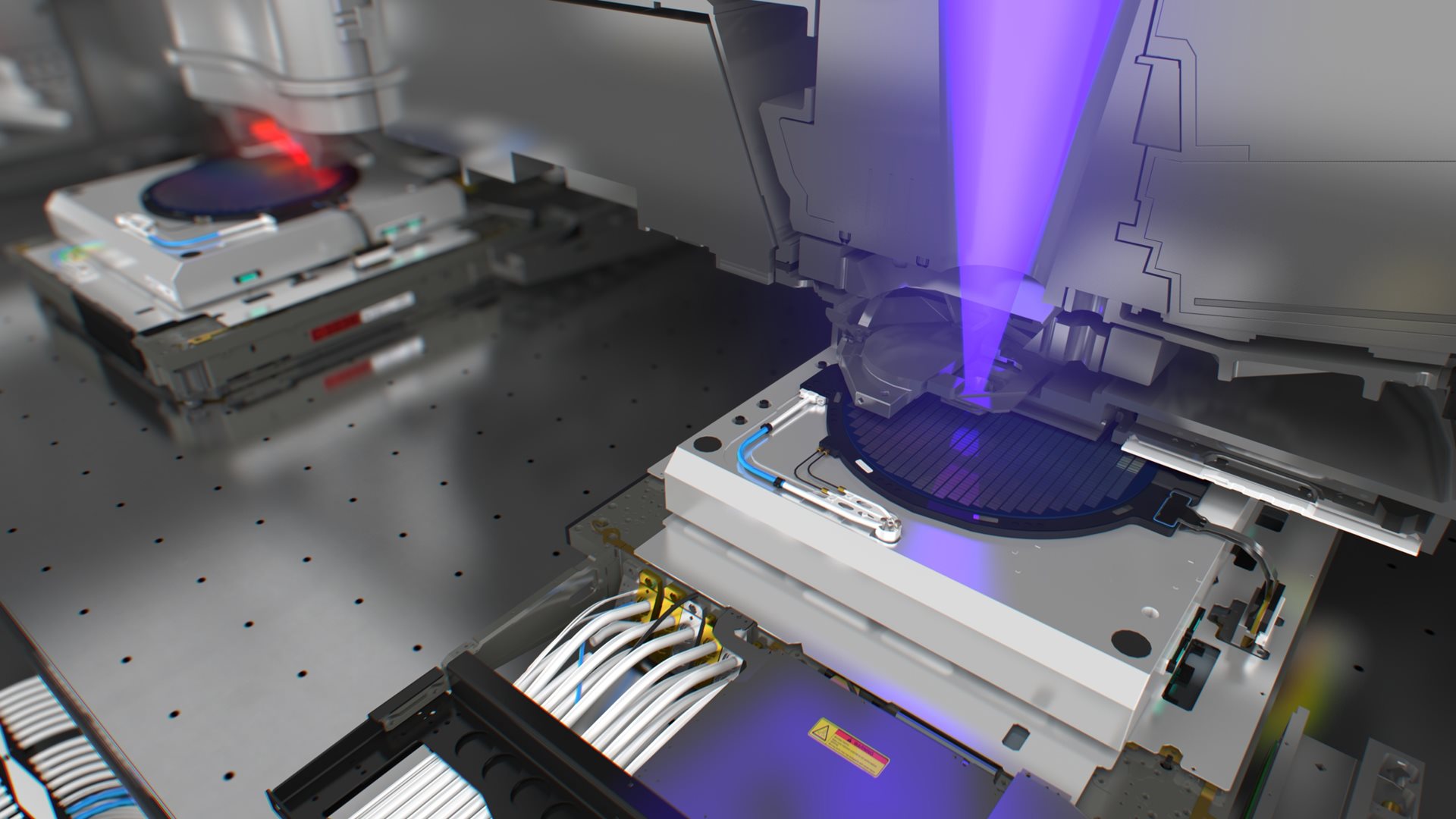
ASML today announced the first customer installation of its HMI eScan 1100, the first multiple e-beam (multibeam) wafer inspection system for in-line yield enhancement applications, including voltage contrast defect inspection and physical defect inspection.
With 25 beams (5x5), the eScan 1100 is able to increase throughput by up to 15 times compared to single e-beam inspection systems that are currently used. It delivers the sensitivity and speed customers need to cover a wide range of defect types in R&D for process development, and in high-volume manufacturing for excursion monitoring.
“The eScan 1100 project really started when ASML and HMI recognized a market gap in defect inspection at the leading-edge technology nodes,” said Yu Cao, CEO of HMI, an ASML company. “There is a need for more accurate defect inspection to capture small defects down to sub 10 nm in size with high throughput for sufficient wafer area coverage. The eScan 1100 multibeam system fills that gap.”
The eScan 1100’s proprietary die-to-database defect inspection capability enables further enhancements in sensitivity and throughput for the most demanding applications such as EUV mask defect monitoring by using wafer print check. The eScan 1100 can detect defects currently overlooked by optical inspection systems in a fraction of the time that it takes single e-beam solutions.
“In May 2020, HMI shipped the first eScan 1000, which was a critical technology demonstrator that yielded strong application learnings and design improvements,” said Gary Zhang, Head of Product Marketing at HMI. “The eScan 1100 incorporates those learnings with an improved electron optical system at a higher resolution and a high-speed stage to increase the system’s overall throughput. In addition, a high-speed computational architecture processes the streams of data from the multiple beamlets in real time.”
About ASML

