Press release - San Jose, California, May 28, 2020
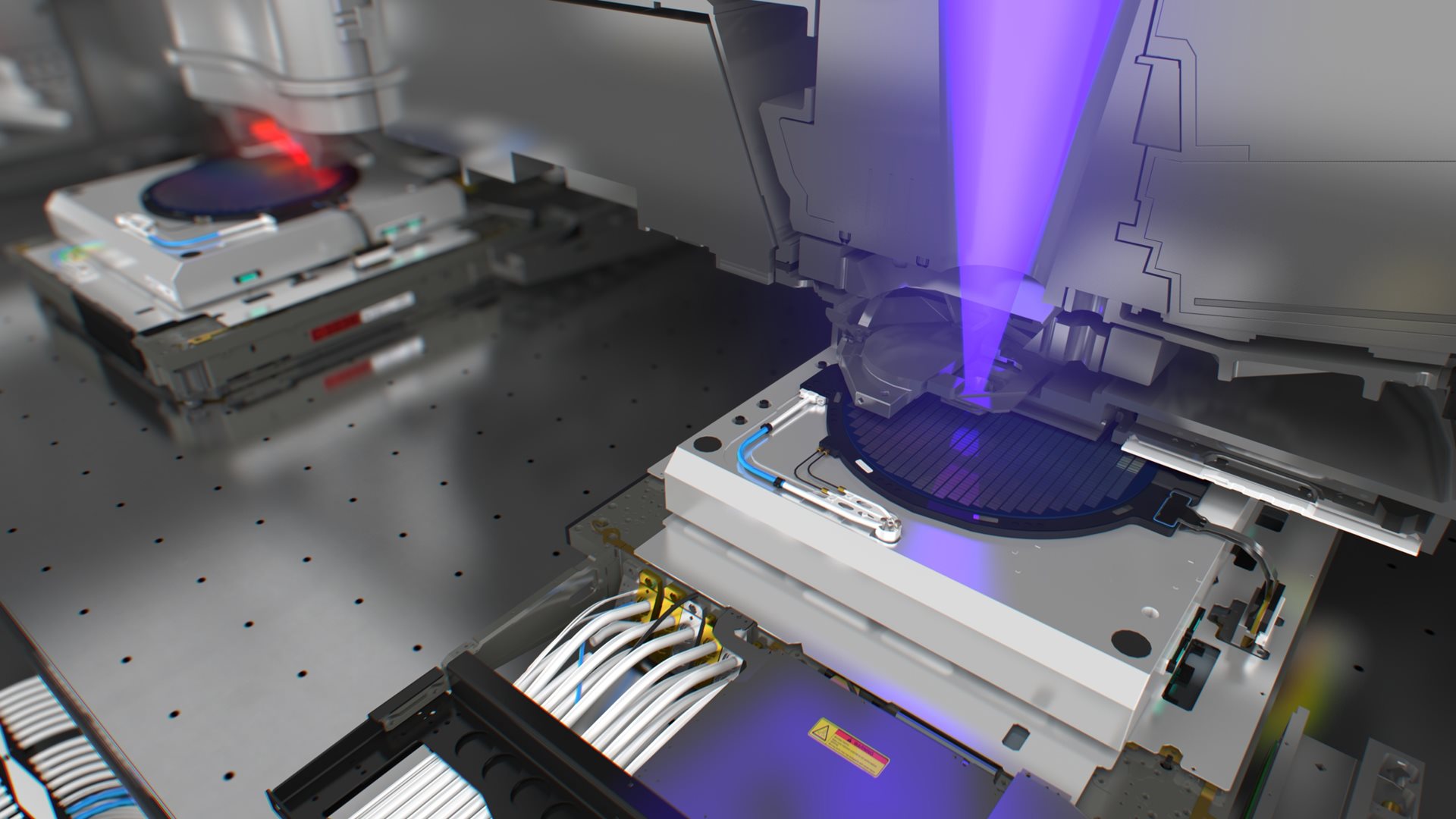
ASML Holding NV (ASML) today announced that it has completed system integration and testing of its first-generation HMI multibeam inspection (MBI) system for 5 nm nodes and beyond. The HMI eScan 1000 demonstrated successful multibeam operation, simultaneously scanning nine beams on a number of test wafers. With nine beams, the eScan 1000 will increase throughput up to 600% compared to single e-beam inspection tools for targeted in-line defect inspection applications.
The new MBI system includes an electron optics system capable of creating and controlling multiple primary electron beamlets and then collecting and processing the resulting secondary electron beams, limiting beam-to-beam crosstalk to less than 2% and delivering consistent imaging quality. It also features a high-speed stage to increase the system’s overall throughput and a high-speed computational architecture to process the streams of data from the multiple beamlets in real time.
“As critical dimensions continue to shrink with each new technology, ‘killer’ defects are becoming smaller and smaller, reaching the point where many are no longer detectable with optical inspection,” says Gary Zhang, vice president of HMI Product Marketing at ASML. “Our new multibeam inspection system is able to detect these smaller defects, while addressing previous e-beam throughput constraints to make it more suitable for high-volume manufacturing environments.”
By offering a range of beam currents, the eScan 1000 is suitable for both physical defect inspection and voltage contrast inspection. This allows customers to target a wide range of defect types both in R&D for process development and high-volume manufacturing for excursion monitoring.
Additionally, its proprietary Supernova die-to-database defect detection capability enables chipmakers to monitor for defects on EUV masks using wafer print checks. It detects defects overlooked by optical inspection systems in a fraction of the time that it takes single e-beam solutions for high-volume manufacturing to do so.
The first multibeam inspection system has shipped to a customer this week for qualification. ASML plans to increase the number of beams and beam resolution for future generations to align with chipmakers’ product roadmap requirements.
About ASML


