Press release - Veldhoven, the Netherlands, August 29, 2006
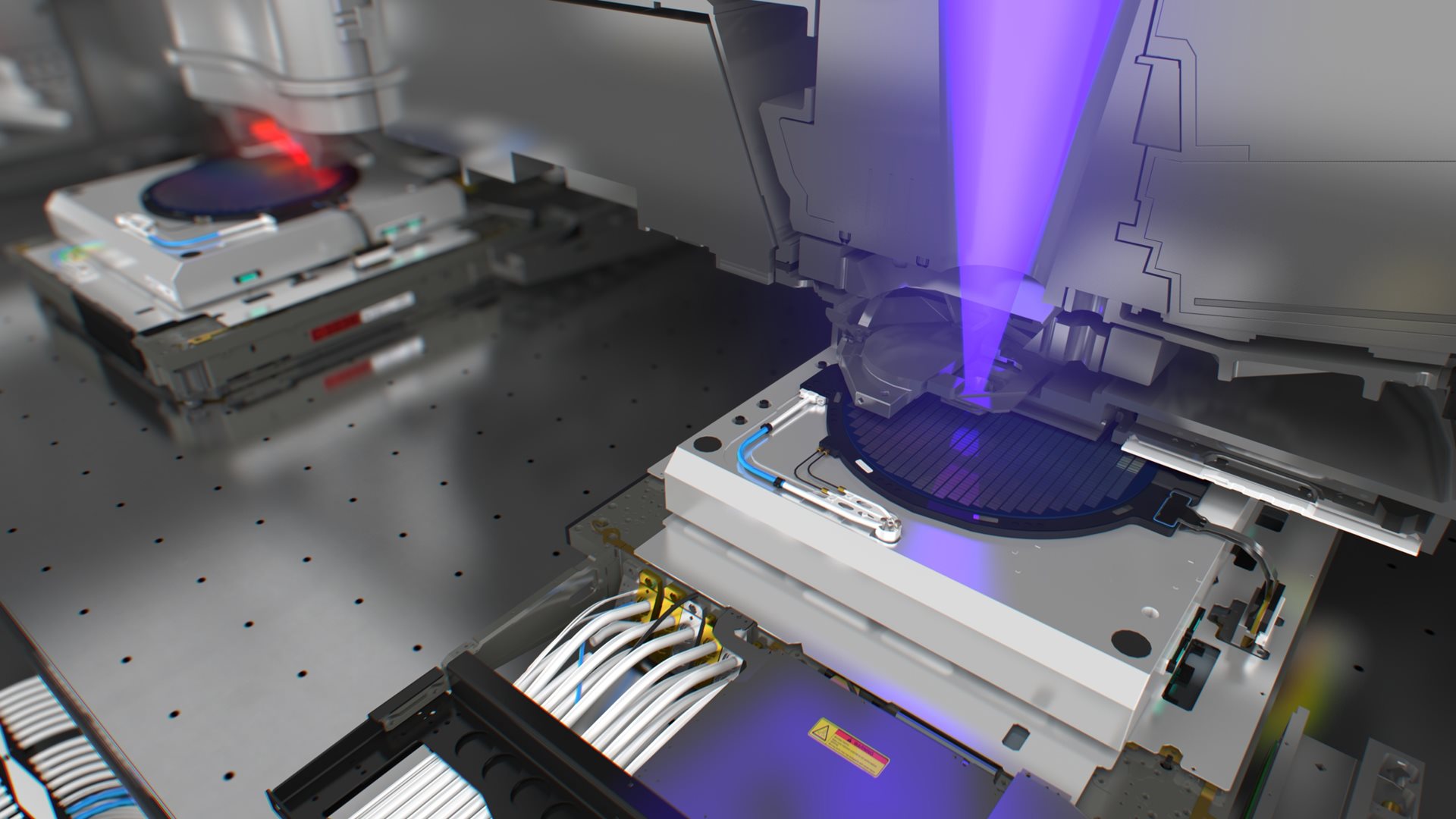
ASML Holding NV (ASML) announced today that it shipped two extreme ultraviolet (EUV) alpha demo tools (ADT) to customers. Both the College of Nanoscale Science and Engineering (CNSE) of the State University of New York (SUNY) at Albany, NY, and the nanoelectronics research institute IMEC in Leuven, Belgium, have received these industry-first, full-field EUV systems. Both institutions will use these R&D tools after installation to conduct ongoing research into this next-generation lithography technology. Shipments were possible after ASML achieved key lithography performance targets including full-field scanning imaging and overlay.
“ASML sets another major industry milestone with the shipment of two full-field EUV lithography systems,” said Martin van den Brink, executive vice president, marketing and technology, ASML. “ASML’s investment in EUV demonstrates our commitment to developing long-term solutions for our customers and maintaining our technology leadership. Many industry partners will now get a chance to work with EUV technology, which should help EUV enter into the next important phase of development. While these tools are research systems, pre-production EUV lithography tools could be shipped as early as 2009 depending on customer commitment.”
ASML has been leading the development of EUV technology. The company considers EUV as the most attractive technology for 32 nm and beyond, because of its potential to be the most cost-effective technology and its extendibility to multiple nodes. Earlier this year at the SPIE Microlithography Conference, the company presented proof-of-concept 35 nm resist images obtained over a full slit of 26 mm, made on one of these systems. ASML expects that these alpha demo tools to be essential in developing the infrastructure for EUV lithography.
“We welcome the delivery of an EUV ADT,” said Luc Van den hove, vice president of Silicon Process and Device Technology at IMEC. “EUV is the most likely candidate technology for the 32 nm half-pitch node. IMEC and its more than 30 lithography program partners have spent much of the last two years in our advanced lithography program working on photoresist for both ArF immersion and EUV lithography. We're eager to expand our program with the integration of an EUV alpha exposure tool.”
“This is a critical step in the development of EUV technology and readying it for eventual commercialization,” said Dr. James Ryan, professor of nanoscience and vice president of technology at CNSE. “With the availability of EUV photomasks and the presence of a critical mass of semiconductor tool suppliers and computer chip manufacturers at CNSE’s Albany NanoTech site, when coupled with ASML's earlier demonstration of operating wafer and reticle stages in a vacuum environment, integration of an alpha exposure tool at CNSE is a logical progression in preparing both the technology and the industry for adopting the EUV technology.”
ASML and its partners will now concentrate on integration of the systems at the customer’s site.
About ASML
About CNSE
About IMEC


