Press release - San Francisco, California, July 12, 2005
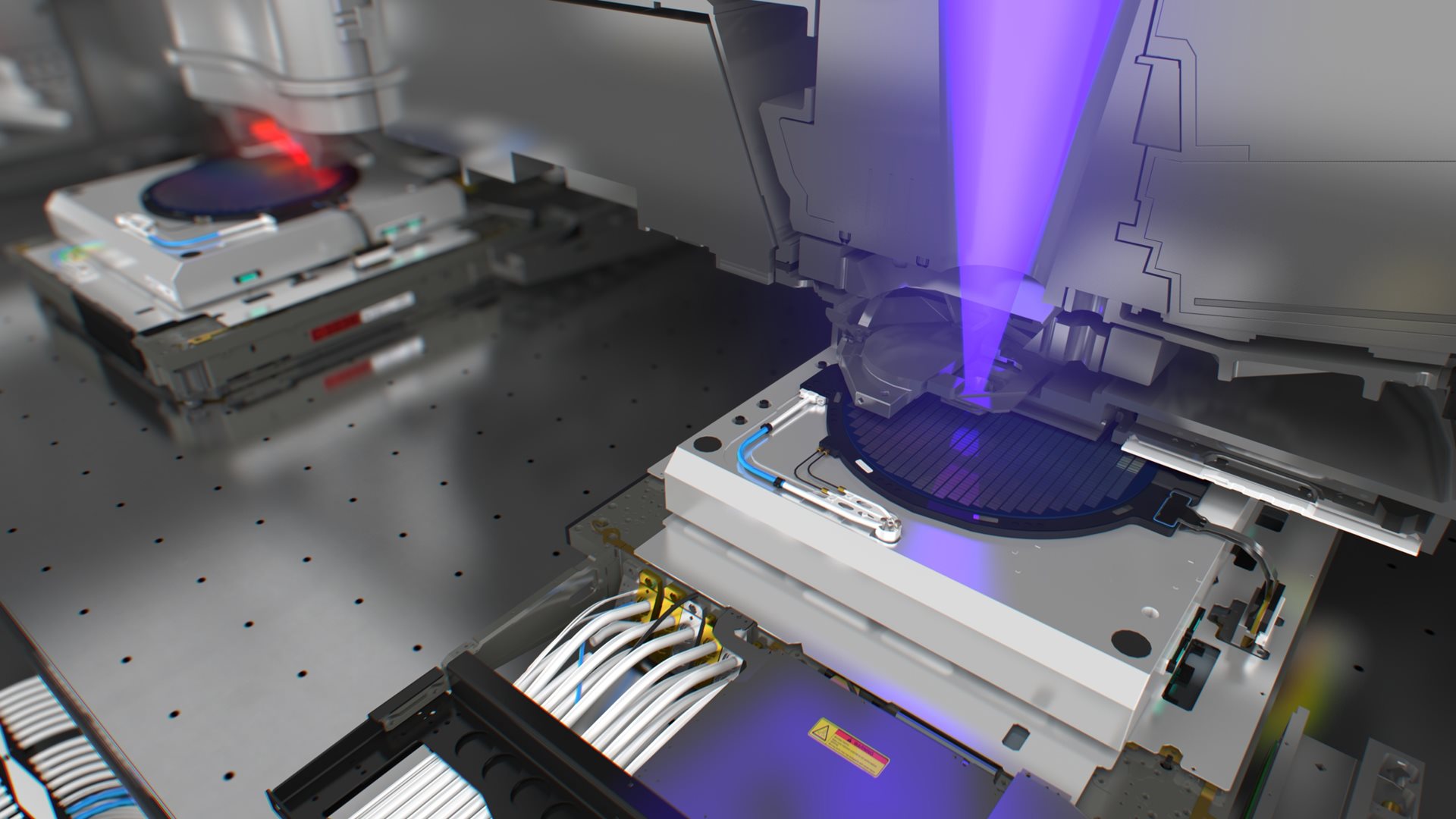
ASML Holding NV (ASML) today announced a new lithography system with the highest numerical aperture (NA) – 1.2 – in the semiconductor industry.1 The ASML TWINSCAN XT:1700i system is a 193 nm immersion scanner capable of volume chip production at the 45 nm node. The new system has a NA that jumped from 0.93 to 1.2, skipping the perceived, pre-immersion barrier of 1.0. The first shipment to a customer, a leading semiconductor manufacturer ordering its second ASML immersion system, will take place in Q1 2006.
The XT:1700i allows chipmakers to improve resolution by 30%, the largest improvement in decades. Better resolution means more chips per wafer or more functionality per chip, thus increasing the value of each wafer. Additionally, the XT:1700i has the highest throughput currently available, 122 wafers per hour, for the 45 nm node.
“The XT:1700i is a milestone for the semiconductor industry. The continuation of Moore’s Law depended on either adapting existing or introducing new technology. ASML was able to enhance its fourth-generation immersion systems with a NA that is unchallenged in the market,” said Martin van den Brink, executive vice president, marketing and technology, ASML.
Additional customer benefits found in the XT:1700i include:
- A new catadioptric lens design which combines refractive components with mirrors to create a hyper NA lens that is cost effective to manufacture and a consistent size with other ASML systems. Co-designed with ASML’s optics partner, Carl Zeiss SMT AG, the new lens will also extend to larger NAs in future products;
- A maximum field size of 26 mm x 33 mm, the largest in the industry;
- A polarized illumination system for improved contrast and exposure latitude at full throughput. With an NA of 1.2, polarization enhances resolution by 5 nm, from 50 to 45 nm;
- A fourth-generation, dual-stage immersion tool. All previous generation tools are being used by real customers to produce real chips.
1 Similar to a camera lens, the numerical aperture – the opening angle of the lens – determines the resolution: the higher the number, the clearer the view. In the case of lithography, higher resolution allows chipmakers to draw more refined features onto silicon wafers. For more information on lithography and definitions of technical terms, please see the ASML technology section of the website.
About ASML


