Press release - Veldhoven, the Netherlands, February 21, 2002
First to market with such technology, ASML marked a record year in 2001 with its leading-edge 193 nm technology products, the 200 mm PAS 5500/1100 and the TWINSCAN AT:1100, also for 300 mm wafer fabrication. Both ASML products incorporate a Carl Zeiss SMT AG ArF Starlith 1100 lens, which features the highest numerical aperture (0.75) available in an ArF lens.
Martin van den Brink, ASML's executive vice president of marketing and technology, said: "Customers are ordering 193 nm lithography systems and we are shipping them. We can do so because our partner Carl Zeiss has 193 nm lenses available both in quality and quantity."
Dr. Hermann Gerlinger, Carl Zeiss Semiconductor Manufacturing Technology's president and CEO, said: "Our production capability can meet any customer demand for 193 nm technology with fast and flexible delivery. Furthermore, our 193 nm lenses have a minimum amount of calcium fluoride, so we are confident about our reliable supply of advanced lenses."
In 2001, Carl Zeiss successfully established a manufacturing operation in Oberkochen, Germany, for production of 193 nm lenses, the critical optical technology for ASML's highest numerical aperture 193 nm ArF imaging of next-generation chips at the 0.10 micron line width.
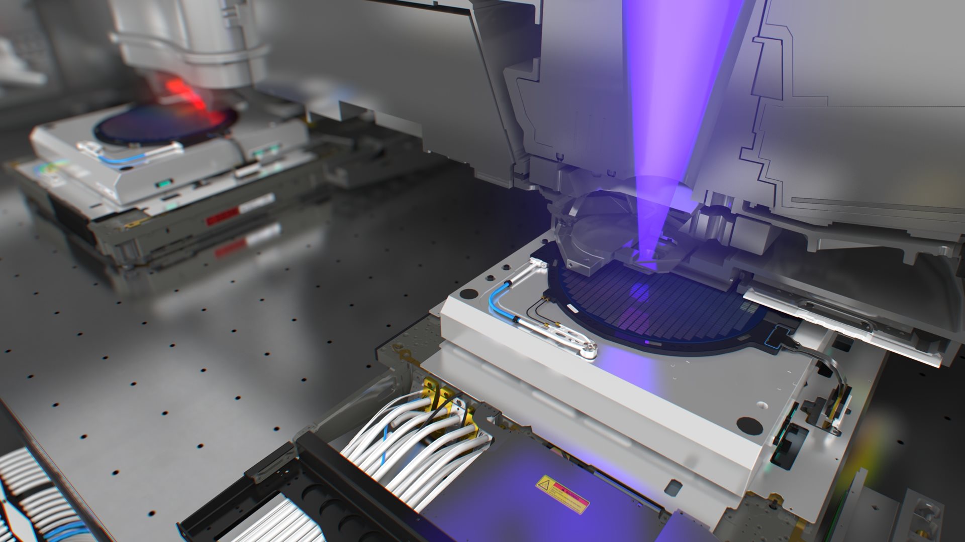
ASML's AT:1100 system builds upon the company's successful 300 mm TWINSCAN dual-stage platform and was developed as the industry's first high-productivity ArF lithography system for volume production applications of 300 mm wafers at the 100 nm technology node. The Starlith's improved aberration control reduces influence on critical lithography structures, which enhances the imaging performance.
ASML's Martin van den Brink added: "Customer demand for 193 nm imaging solutions is growing and we have sufficient supply. We made a commitment to our customers to provide industry-leading productivity for 100 nm volume manufacturing. We are delivering."
About ASML
About Carl Zeiss SMT AG


