Press release - San Francisco, California, July 10, 2000
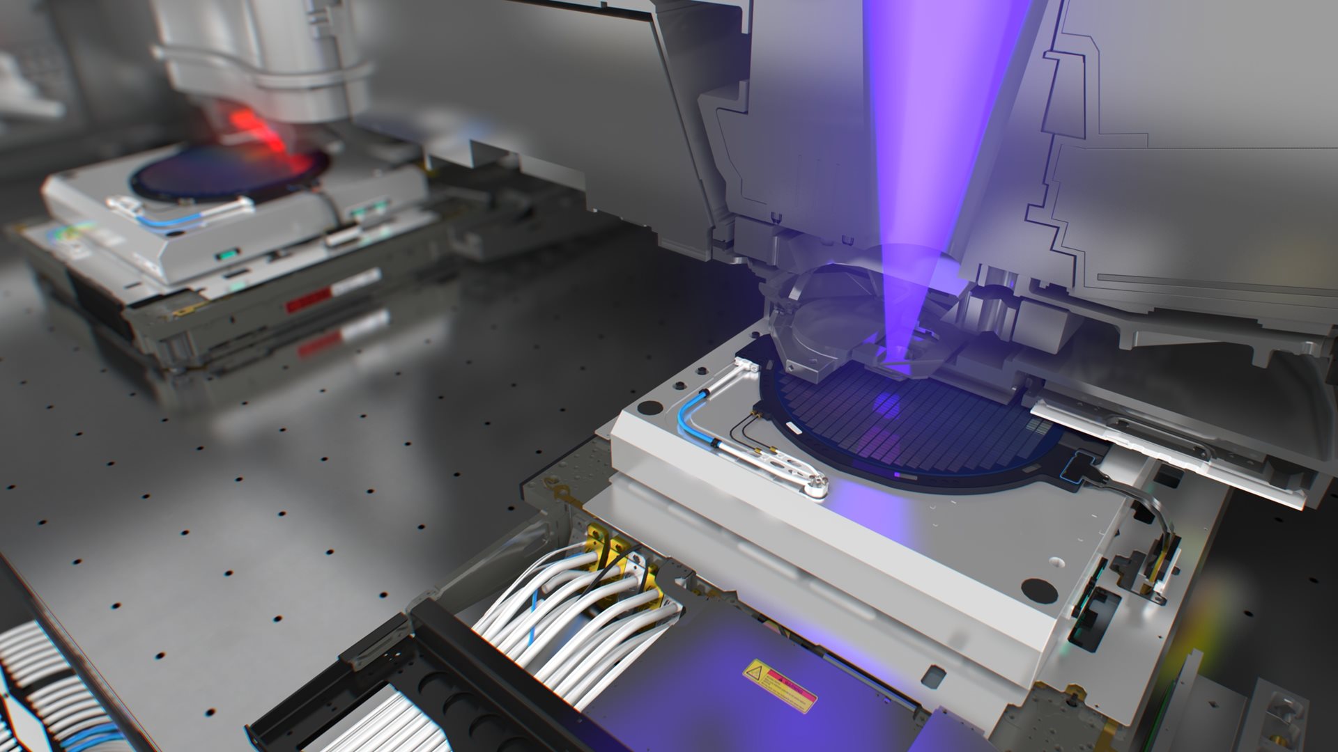
A new 300 mm lithography platform enabling the highest productivity at the limits of optical technology has been announced by ASML, a world leader in semiconductor photolithography systems. The new platform and the first system in this new product family, the AT:700S scanner, were introduced today at the annual SEMICON West trade show. The platform, named TWINSCAN, is the result of a collaborative development program that was started over four years ago by ASML and its strategic technology partners. The TWINSCAN platform blends significant innovations in system architecture and key components with the proven imaging performance of Carl Zeiss Starlith optics.
"The TWINSCAN platform delivers on the market need for a platform to support mass production capability on 300 mm substrates down to the 70 nm ITRS node," said Martin van den Brink, ASML's executive vice president of marketing and technology. "This platform will set new standards with respect to imaging accuracy and productivity for 300 mm lithography systems."
Improvements in imaging and productivity were two of the most important drivers in developing TWINSCAN. Designing and engineering high-speed 300 mm stages, with their greater mass, posed a substantial challenge to vibration control. TWINSCAN uses a novel 'balance mass' system designed to effectively eliminate stage-induced system vibration, thereby increasing focus budgets and image contrast. Further improvements reduce sensitivity to environmental disturbances including temperature variations, thus helping to extend TWINSCAN's imaging to sub-100 nm design rules. TWINSCAN's design is set to surpass existing productivity levels, with an ultimate 300 mm wafer throughput capability well in excess of 100 wafers per hour. This performance will be achieved through a variety of technological advancements that will be incorporated in the TWINSCAN product range over time. These will include significant developments now underway in wafer and reticle stages, optics, lasers, robotics and metrology. TWINSCAN was timed to address the semiconductor industry's current adoption of 300 mm wafers in volume production and to accommodate future lithographic technologies. It is designed to handle 200 mm or 300 mm wafers and to support optics for i-line (365 nm), deep UV (248 nm), 193 nm and 157 nm wavelengths.
"Given the high level of investment for 300 mm fabs, our customers are placing a high priority on selecting solutions that provide the best long-term value of ownership," said Dave Chavoustie, ASML's executive vice president of worldwide sales. "We are currently witnessing a high level of interest in this new technology from many of the world's top ten IC manufacturers, which include some major new customers for ASML."
ASML expects to begin shipping the first TWINSCAN systems in the third quarter of this year. The AT:700S, the first model in this new product family, has a list price starting at €9.1 million.
About ASML
Forward-looking statements


