Press release - Tokyo, Japan, December 6, 2000
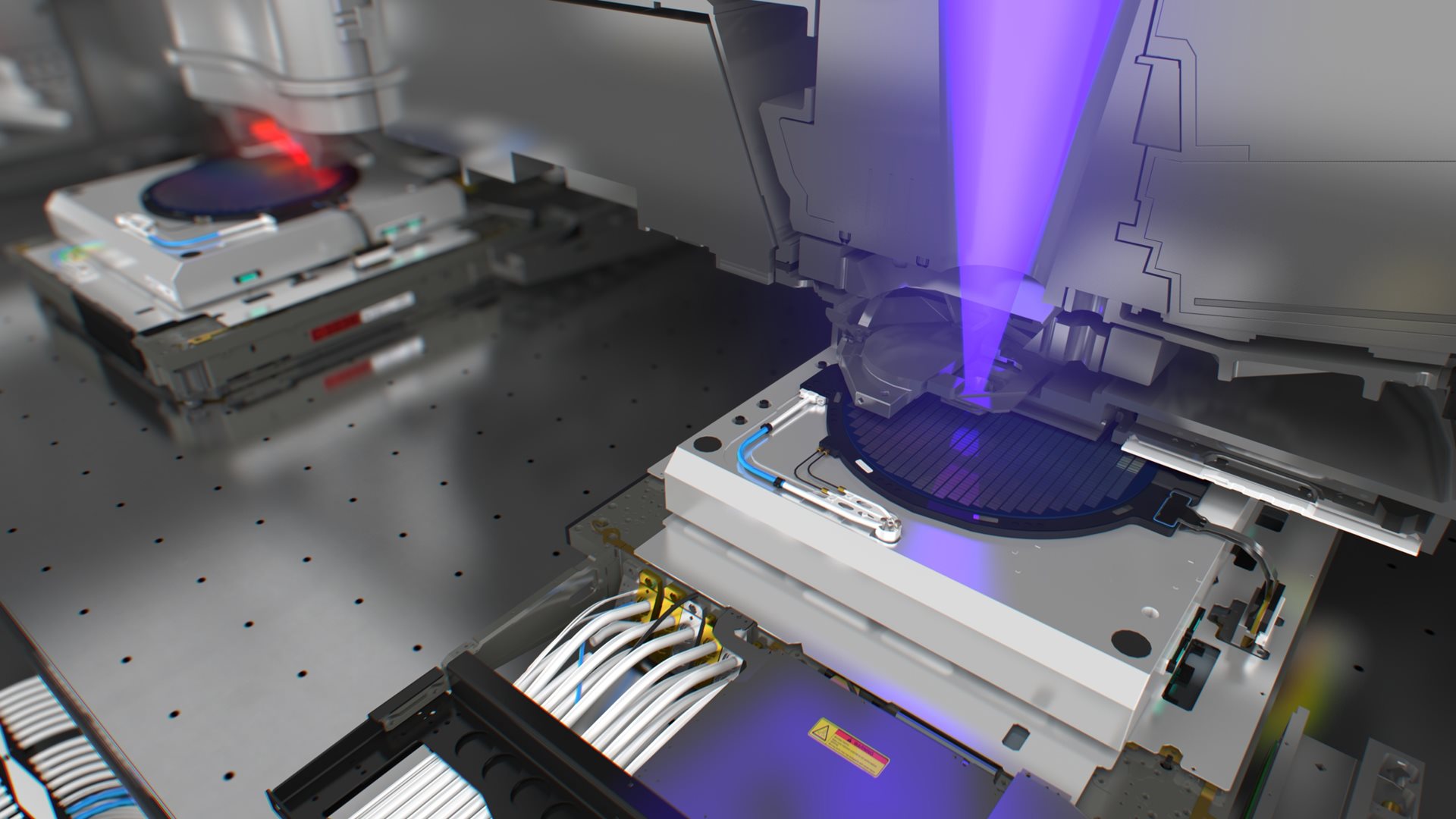
ASML today announces the introduction of dual wafer stage technology for new i-line and deep UV imaging systems, extending the product offerings of its TWINSCAN 300mm technology platform. This dual wafer stage system optimizes the lithographic processing of 300 mm wafers by parallel operation of two independent wafer stages.
"This is the industry's first scanning lithography system to incorporate two wafer stages," said Martin van den Brink, executive vice president for marketing and technology of ASML. He further explains that "TWINSCAN exposes one wafer, while in parallel the next wafer is being aligned and its surface mapped with interferometer precision."
When imaging is completed on the first wafer, the two stages are swapped and the next aligned wafer moves into the exposure position. This eliminates virtually all overhead time, allowing continuous patterning of product wafers for maximum productivity. ASML offers this dual wafer stage capability on two new systems, the AT:750 KrF system and the AT:400 i-line tool, to allow IC makers to implement cost-effective mix-and-match strategies for the lowest production costs. The TWINSCAN 300 mm platform, introduced by ASML in July, is designed to extend optical lithography to its limits and will ultimately support not only i-line (365 nm wavelength light) and KrF (248 nm), but also ArF (193 nm) and 157 nm technologies. With the new systems, ASML is realizing the productivity advantage that the TWINSCAN platform offers. The dual 300 mm wafer stages operating at high speeds require higher acceleration forces that, without proper measures, would pose a substantial challenge in vibration control. TWINSCAN's 'balance mass' system effectively eliminates stage-induced vibration, which increases focus budgets and image contrast. In addition, fundamental improvements at the system level provide the temperature and environmental control needed to achieve the overlay performance required for design rules down to 70nm and beyond.
"Our dual-stage platform demonstrates ASML's commitment to delivering the most advanced lithography equipment, which is especially timely as our customers begin to ramp up their 300mm fabs," said Dave Chavoustie, ASML's executive vice president of worldwide sales. "IC makers worldwide clearly recognize the productivity advantage enabled by TWINSCAN."
The TWINSCAN dual wafer stage systems are capable of processing 300 mm wafers at speeds up to 120 wafers per hour. The KrF AT:750 is guaranteed for 130 nm resolution with 20 nm overlay accuracy and has a numerical aperture that is adjustable anywhere from 0.50 to 0.70 for optimal process latitude. The AT:400 i-line system is specified for 280 nm resolution with 25 nm overlay accuracy. This product's numerical aperture is adjustable between 0.48 and 0.65. Both tools use Carl Zeiss' Starlith 4X reduction lenses with imaging field sizes of 26 mm x 32 mm. This enables cost-effective mix-and-match manufacturing performance. ASML will begin shipping its first dual-stage units in the middle of 2001.
About ASML


