Press release - Tokyo, Japan, December 5, 2001
ASML today introduced the industry's first KrF (248 nm) Step & Scan 300 mm dual-stage lithography system capable of 110 nm resolution. The TWINSCAN AT:850B features Carl Zeiss Starlith 850 advanced projection optics with a numerical aperture (NA) of 0.80, which is the highest NA available in a KrF system.
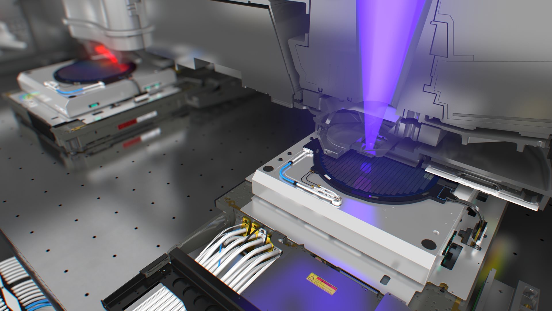
The AT:850B has an industry-leading throughput of 95 300 mm wafers per hour and is the latest addition to ASML's TWINSCAN dual-stage 300 mm lithography platform. With two stages working simultaneously, this platform allows wafer alignment and leveling to take place while another wafer is being exposed, providing a major boost in productivity and accuracy. The separation of the alignment and leveling stage from the exposure operation virtually eliminates non-productive overhead time while ensuring precision in manufacturing. The first AT:850B system will ship this month to a major customer in Asia.
ASML expects the AT:850B to be a high volume production system used for a broad range of device manufacturing, including very advanced memory and logic production at 110 nm and below design rules. The same Starlith 850 high numerical aperture projection optics is also available in ASML's high-performance 200 mm lithography system, the PAS 5500/850B™. With the addition of the TWINSCAN AT:850B and the PAS 5500/850B systems, ASML now offers the best value of ownership solution for either 300 mm or 200 mm wafer fab production with the highest NA at each manufacturing technology – i-line, KrF and ArF.
"These new high NA systems are the first to enable the volume production of chips with 110 nm feature sizes using KrF technology," said Martin van den Brink, executive vice president of ASML Marketing and Technology. "By extending production proven KrF technology we are providing our customers with a powerful cost effective means to shrink existing chip designs and bring the most advanced chips to market faster."
About ASML


