
CD = k1 • λ / NA
Rayleigh criterion equation
In the Rayleigh criterion equation, CD is the critical dimension, or smallest possible feature size, and λ is the wavelength of light used.
NA is the numerical aperture of the optics, defining how much light they can collect.
Finally, k1 (or the k1 factor) is a coefficient that depends on many factors related to the chip manufacturing process. The physical limit lithography is k1 = 0.25.
Smaller critical dimension can be achieved by using a combination of smaller light wavelength and larger numerical aperture (NA), while pushing k1 as close as possible to the physical limit.

The limits of small
Much of the R&D in the semiconductor industry is focused on reducing critical dimension. ASML’s lithography machines print at extremely high resolution, helping chipmakers to decrease this critical dimension further.
More advanced microchips mean smaller features, which need shorter wavelengths of light, more powerful lenses and / or a lower k1 factor. Reducing the light wavelength is a major technology shift that requires new lithography machines with new light sources – as well as new (optical and resist) materials and new processes. But it also brings the biggest strides forward in in chip performance.
In between these wavelength steps, progress in the industry is driven by lens development and reducing k1 through clever tweaks to the lithography process and techniques such as computational lithography.
LITHOGRAPHY PRINCIPLES
The science behind the chip


More about ASML technology
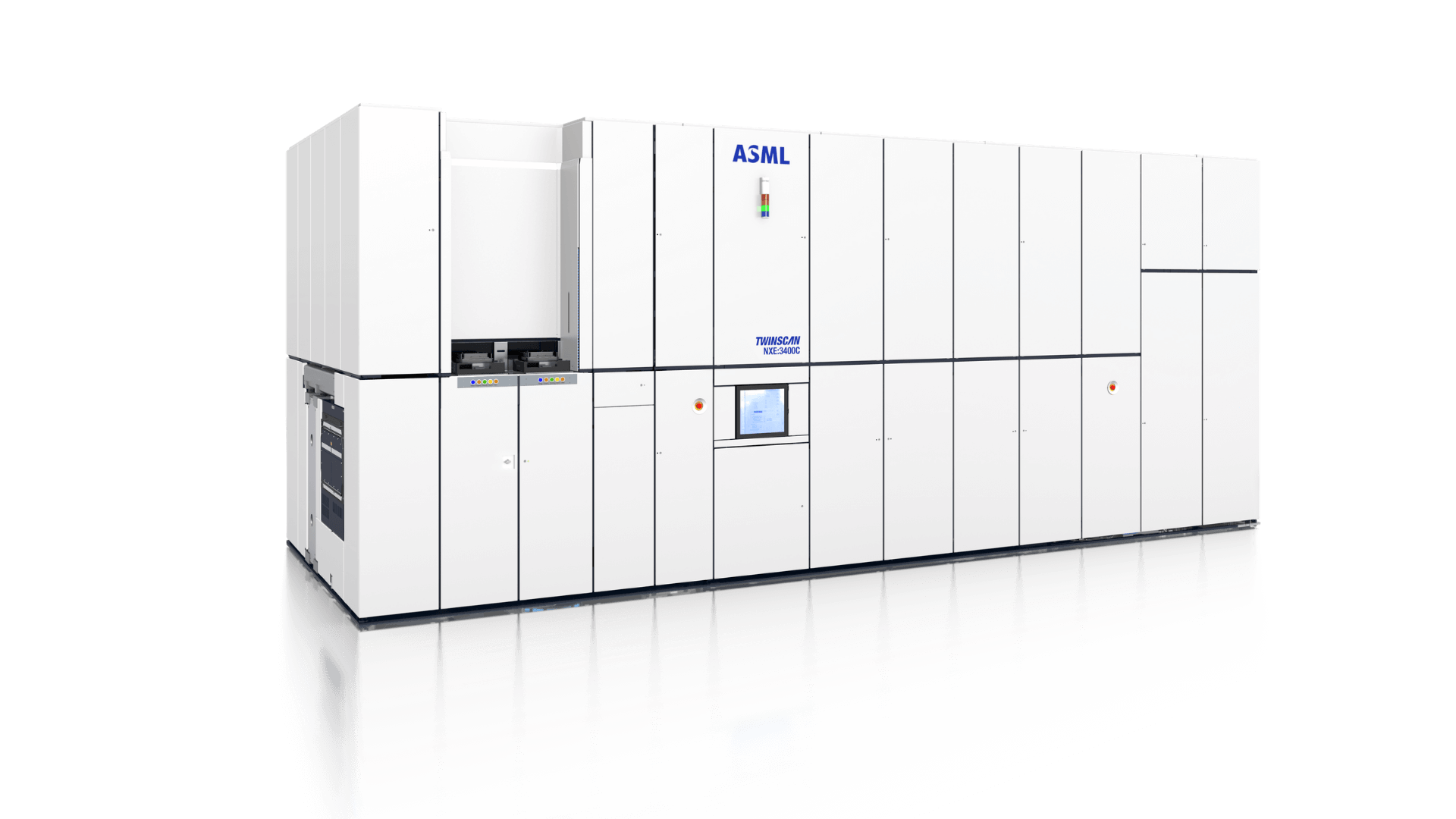 EUV lithography systems
Providing highest resolution in high-volume manufacturing, ASML’s extreme ultraviolet lithography machines are pushing Moore’s Law forward.
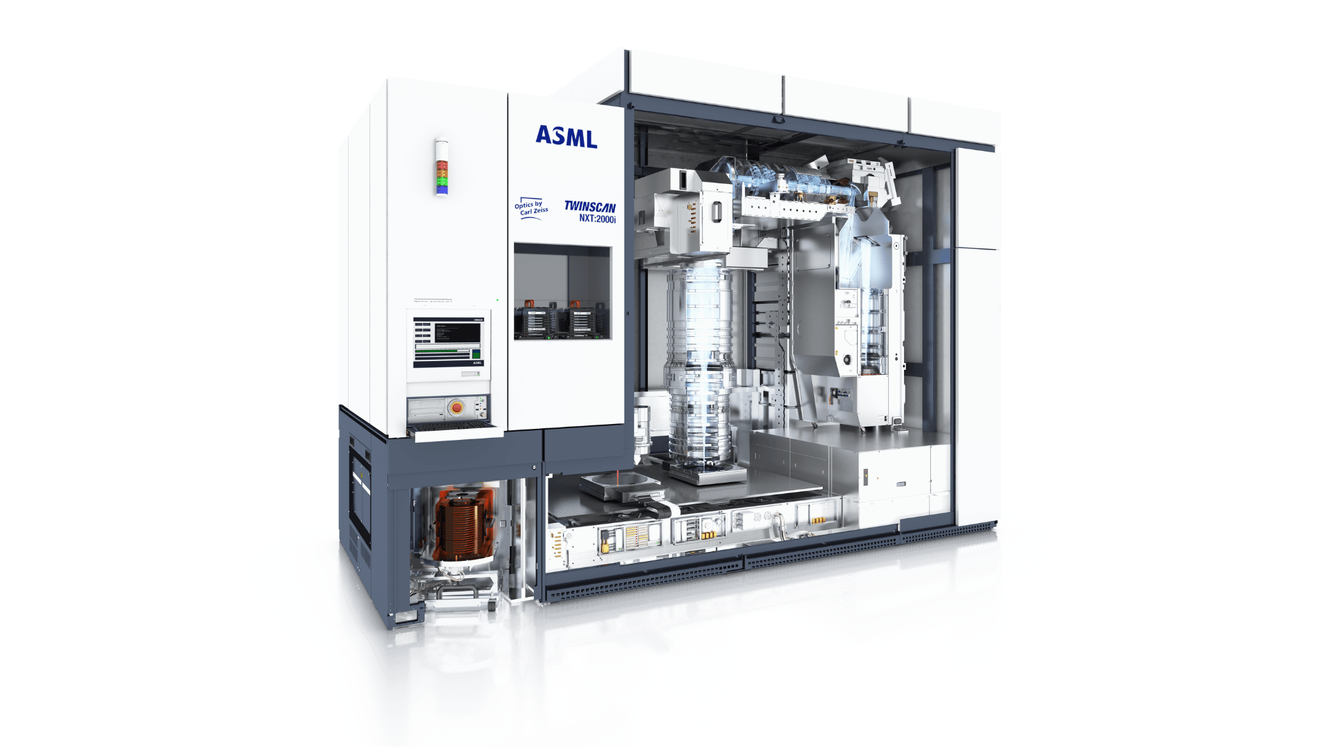 DUV lithography systems
ASML's deep ultraviolet (DUV) lithography systems dive deep into the UV spectrum to print the tiny features that form the basis of the microchip.
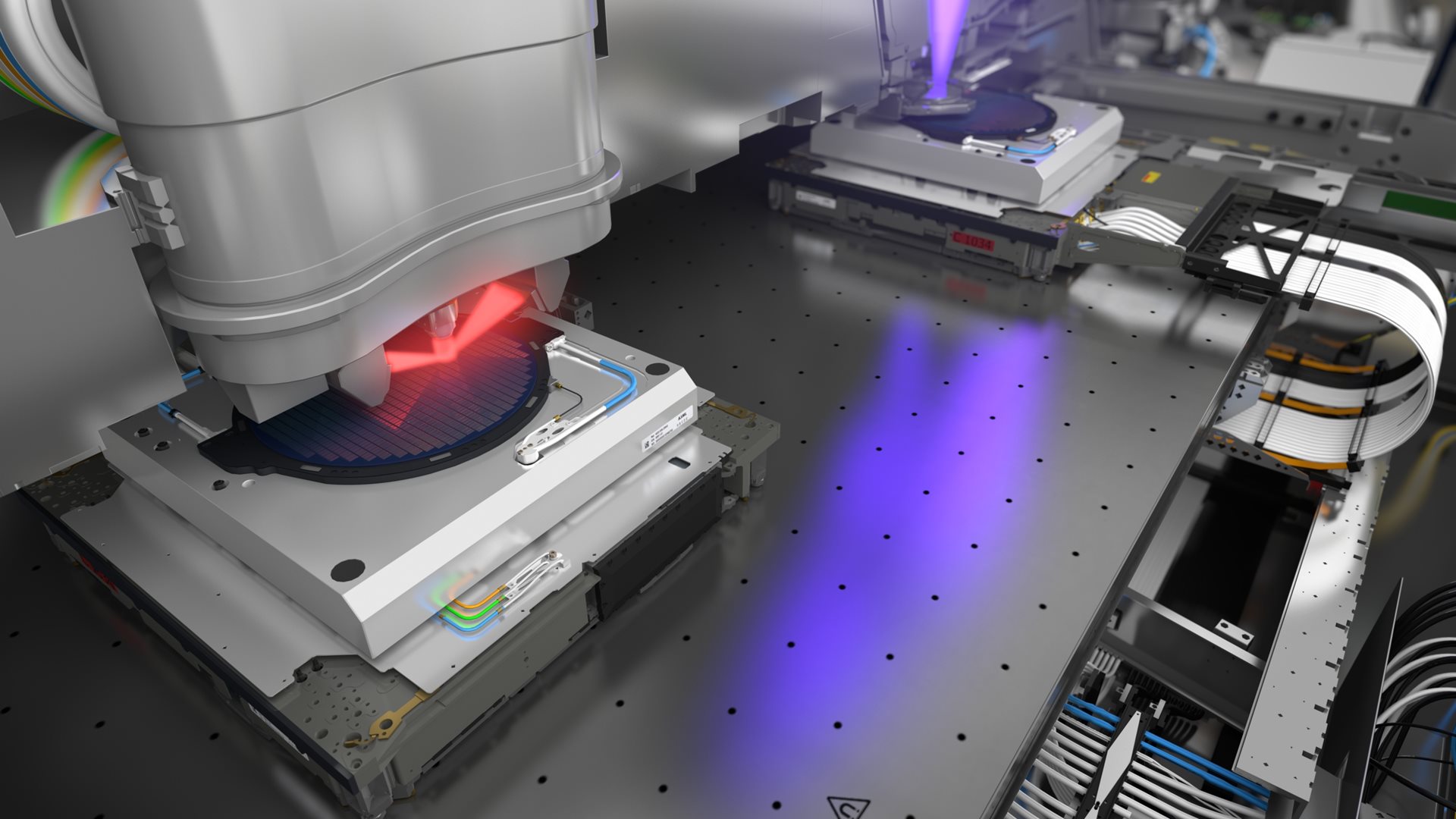 Metrology and inspection systems
Delivering speed and accuracy, our metrology and inspection portfolio covers every step manufacturing processes, from R&D to mass production.
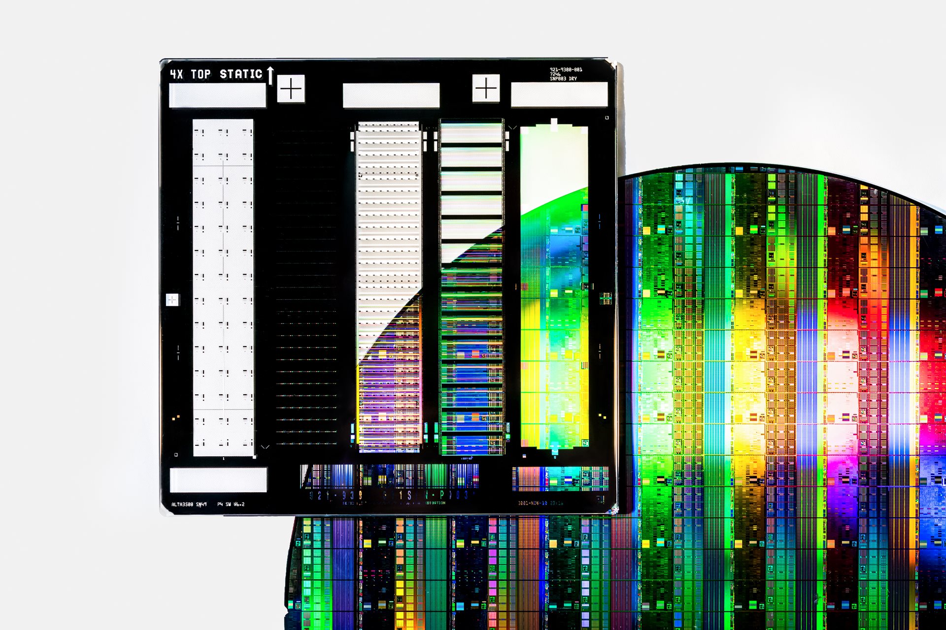 Computational lithography
ASML's industry-leading computational lithography products enable accurate lithography simulations that help to improve chip yield and quality.